
Datasheet


SLOS175B − FEBRUARY 1997 − REVISED JANUARY 2008
44
POST OFFICE BOX 655303 • DALLAS, TEXAS 75265
TYPICAL CHARACTERISTICS
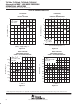
−500 −300 −100
V
IO
− Input Offset Voltage − µV
12
8
4
0
100
Percentage of Units − %
16
20
300 500
DISTRIBUTION OF TLC2201
INPUT OFFSET VOLTAGE
408 Units Tested From 2 Wafer Lots
V
DD±
= ±5 V
T
A
= 25°C
P Package
Figure 5
Figure 6
8
6
2
0
−1000 200
Percentage of Units − %
10
14
16
600 1000
4
12
TLC2202
DISTRIBUTION OF
INPUT OFFSET VOLTAGE
V
IO
− Input Offset Voltage − µV
V
DD±
= ±15 V
1726 Amplifiers Tested From 1 Wafer Lot
−600 −200
T
A
= 25°C
P Package
Figure 7
−5
0
8
IIB − Input Bias Current − pA
4
2
6
INPUT BIAS CURRENT
vs
COMMON-MODE INPUT VOLTAGE
10
−2
−4
−6
−8
−10
−4−3−2−1012345
V
IC
− Common-Mode Input Voltage − V
I
IB
V
DD±
= ±5 V
T
A
= 25°C
Figure 8
150
100
50
0
25 45 65 85
200
250
300
105 125
INPUT BIAS CURRENT
†
vs
FREE-AIR TEMPERATURE
− Input Bias Current − pA
I
IB
T
A
− Free-Air Temperature − °C
V
O
= 0
V
IC
= 0
V
DD±
= ±5 V
†
Data at high and low temperatures are applicable only within the rated operating free-air temperature ranges of the various devices.