
Datasheet


SLOS175B − FEBRUARY 1997 − REVISED JANUARY 2008
43
POST OFFICE BOX 655303 • DALLAS, TEXAS 75265
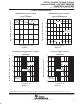
TYPICAL CHARACTERISTICS
Table of Graphs
FIGURE
V
IO
Input offset voltage Distribution 5, 6
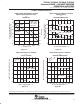
I
IB
Input bias current
vs Common-mode input voltage
7
I
IB
Input bias current
vs Common-mode input voltage
vs Free-air temperature
7
8
V
OM
Maximum peak output voltage
vs Output current
9
V
OM
Maximum peak output voltage
vs Output current
vs Free-air temperature
9
10
V
O(PP)
Maximum peak-to-peak output voltage vs Frequency 11
vs Frequency
12
V
OH
High-level output voltage
vs Frequency
vs High-level output current
12
13
V
OH
High-level output voltage
vs High-level output current
vs Free-air temperature
13
14
V
OL
Low-level output voltage
vs Low-level output current
15
V
OL
Low-level output voltage
vs Low-level output current
vs Free-air temperature
15
16
A
VD
Large-signal differential voltage amplification
vs Frequency
17
A
VD
Large-signal differential voltage amplification
vs Frequency
vs Free-air temperature
17
18
I
OS
Short-circuit output current
vs Supply voltage
19
I
OS
Short-circuit output current
vs Supply voltage
vs Free-air temperature
19
20
CMRR Common-mode rejection ratio vs Frequency 21
I
DD
Supply current
vs Supply voltage
22
I
DD
Supply current
vs Supply voltage
vs Free-air temperature
22
23, 24
Pulse response
Small signal
25, 26
Pulse response
Small signal
Large signal
25, 26
27, 28
SR
Slew rate
vs Supply voltage
29
SR Slew rate
vs Supply voltage
vs Free-air temperature
29
30
Noise voltage (referred to input)
0.1 to 1 Hz
31
Noise voltage (referred to input)
0.1 to 1 Hz
0.1 to 10 Hz
31
32
Gain-bandwidth product
vs Supply voltage
33, 34
Gain-bandwidth product
vs Supply voltage
vs Free-air temperature
33, 34
35
φ
m
Phase margin
vs Supply voltage
36, 37
φ
m
Phase margin
vs Supply voltage
vs Free-air temperature
36, 37
38, 39
Phase shift vs Frequency 17