
Datasheet


SLOS175B − FEBRUARY 1997 − REVISED JANUARY 2008
27
POST OFFICE BOX 655303 • DALLAS, TEXAS 75265
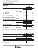
TLC2202I electrical characteristics at specified free-air temperature, V
DD
= 5 V (unless otherwise
noted)
PARAMETER
TEST CONDITIONS
T
A
†
TLC2202AI TLC2202BI
UNIT
PARAMETER
TEST CONDITIONS
T
A
†
MIN TYP MAX MIN TYP MAX
UNIT
V
IO
Input offset voltage
25°C 80 500 80 500
µV
V
IO
Input offset voltage
Full range 700 700
µ
V
α
VIO
Temperature coefficient of
Full range
0.5
0.5
µV/°C
α
VIO
Temperature coefficient of
input offset voltage
Full range
0.5
0.5
µ
V/
°
C
Input offset voltage long-term
drift (see Note 4)
V
IC
= 0, R
S
= 50 Ω
25°C
0.001 0.005 0.001 0.005 µV/mo
I
IO
Input offset current
25°C 0.5 60 0.5 60
pA
I
IO
Input offset current
Full range 150 150
pA
I
IB
Input bias current
25°C 1 60 1 60
pA
I
IB
Input bias current
Full range 150 150
pA
Common-mode input
0
0
V
ICR
Common-mode input
voltage range
R
S
= 50 Ω Full range
0
to
0
to
V
V
ICR
voltage range
R
S
= 50 Ω
Full range
to
2.7
to
2.7
V
V
OH
Maximum high-level output
R
L
= 10 kΩ
25°C 4.7 4.8 4.7 4.8
V
V
OH
Maximum high-level output
voltage
R
L
= 10 k
Ω
Full range 4.7 4.7
V
V
OL
Maximum low-level output
I
O
= 0
25°C 0 50 0 50
mV
V
OL
Maximum low-level output
voltage
I
O
= 0
Full range 50 50
mV
V
O
= 1 V to 4 V,
25°C 150 315 150 315
A
VD
Large-signal differential
V
O
= 1 V to 4 V,
R
L
= 500 kΩ
Full range 100 100
V/mV
A
VD
Large-signal differential
voltage amplification
V
O
=1 V to 4 V,
25°C 25 55 25 55
V/mV
voltage amplification
V
O
=1 V to 4 V,
R
L
= 10 kΩ
Full range 15 15
CMRR
Common-mode rejection ratio
V
IC
= V
ICR
min,
25°C 75 110 75 110
dB
CMRR
Common-mode rejection ratio
V
IC
= V
ICR
min,
V
O
= 0, R
S
= 50 Ω
Full range 75 75
dB
k
SVR
Supply-voltage rejection ratio
V
DD
= 4.6 V to 16 V
25°C 80 110 80 110
dB
k
SVR
Supply-voltage rejection ratio
(∆V
DD±
/∆V
IO
)
V
DD
= 4.6 V to 16 V
Full range 80 80
dB
I
DD
Supply current
V
O
= 2.5 V,
No load
25°C 1.7 2.6 1.7 2.6
mA
I
DD
Supply current
V
O
= 2.5 V,
No load
Full range 2.6 2.6
mA
†
Full range is −40°C to +85°C
NOTE 4: Typical values are based on the input offset voltage shift observed through 168 hours of operating life test at T
A
= 150°C extrapolated
to T
A
= 25°C using the Arrhenius equation and assuming an activation energy of 0.96 eV.
TLC2202I operating characteristics at specified free-air temperature, V
DD
= 5 V
PARAMETER
TEST CONDITIONS
T
A
†
TLC2202AI TLC2202BI
UNIT
PARAMETER
TEST CONDITIONS
T
A
†
MIN TYP MAX MIN TYP MAX
UNIT
V
O
= 0.5 V to 2.5 V,
25°C
1.6
2.5
1.6
2.5
SR
Slew rate at unity gain
V
O
= 0.5 V to 2.5 V,
25
°
C
1.6
2.5
1.6
2.5
V/ s
SR Slew rate at unity gain
V
O
= 0.5 V to 2.5 V,
R
L
= 10 kΩ,C
L
= 100 pF
Full range 1 1
V/µs
V
n
Equivalent input noise voltage
f = 10 Hz 25°C 18 35 18 30
nV/√Hz
V
n
Equivalent input noise voltage
(see Note 5)
f = 1 kHz
25°C 8 15 8 12
nV/√Hz
V
N(PP)
Peak-to-peak equivalent
f = 0.1 to 1 Hz 25°C 0.5 0.5
µV
V
N(PP
)
Peak-to-peak equivalent
input noise voltage
f = 0.1 to 10 Hz
25°C 0.7 0.7
µ
V
I
n
Equivalent input noise current 25°C 0.6 0.6
fA/√Hz
Gain-bandwidth product
f = 10 kHz, R
L
= 10 kΩ
25 C
1.9
1.9
MHz
Gain-bandwidth product
f = 10 kHz, R
L
= 10 kΩ
,
C
L
= 100 pF
25
°
C
1.9
1.9
MHz
Gain-bandwidth product
L
C
L
= 100 pF
25 C
1.9
1.9
MHz
φ
m
Phase margin at unity gain
R
L
= 10 kΩ,C
L
= 100 pF
25°C
47°
47°
φ
m
Phase margin at unity gain
R
L
= 10 k
Ω
,C
L
= 100 pF
25
°
C
47
°
47
°
†
Full range is −40°C to +85°C
NOTE 5: This parameter is tested on a sample basis for the TLC2202A and on all devices for the TLC2202B. For other test requirements, please
contact the factory. This statement has no bearing on testing or nontesting of other parameters.