
Datasheet


SLVS461B − JANUARY 2003 − REVISED JULY 2003
2
POST OFFICE BOX 655303 • DALLAS, TEXAS 75265
description/ordering information (continued)
Quality, low-cost, bipolar fabrication with innovative design concepts is employed for the TL3474, TL3474A
operational amplifiers. These devices offer 4 MHz of gain-bandwidth product, 13-V/µs slew rate, and fast settling
time without the use of JFET device technology. Although the TL3474 and TL3474A can be operated from split
supplies, they are particularly suited for single-supply operation because the common-mode input voltage
range includes ground potential (V
CC−
). With a Darlington transistor input stage, these devices exhibit high input
resistance, low input offset voltage, and high gain. The all-npn output stage, characterized by no dead-band
crossover distortion and large output voltage swing, provides high-capacitance drive capability, excellent phase
and gain margins, low open-loop high-frequency output impedance, and symmetrical source/sink ac frequency
response. These low-cost amplifiers are an alternative to the MC34074/A and MC33074/A operational
amplifiers.
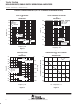
schematic (each amplifier)
V
CC+
OU
T
V
CC−
/GND
IN−
IN+