
Datasheet


TL16C554A, TL16C554AI
ASYNCHRONOUS-COMMUNICATIONS ELEMENT
SLLS509E − AUGUST 2001 − REVISED JUNE 2010
9
POST OFFICE BOX 655303 • DALLAS, TEXAS 75265
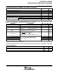
recommended operating conditions, low voltage (3.3-V nominal)
MIN NOM MAX UNIT
Supply voltage, V
CC
3 3.3 3.6 V
Clock high-level input voltage at XTAL1, V
IH(CLK)
2 V
CC
V
Clock low-level input voltage at XTAL1, V
IL(CLK)
−0.5 0.8 V
High-level input voltage, V
IH
2 V
CC
V
Low-level input voltage, V
IL
−0.5 0.8 V
Clock frequency, f
clock
16 MHz
Operating free air temperature T
TL16C554A 0 70 °C
Operating free-air temperature, T
A
TL16C554AI −40 85 °C
electrical characteristics over recommended ranges of operating free-air temperature and supply
voltage, low voltage (3.3-V nominal) (unless otherwise noted)
PARAMETER TEST CONDITIONS MIN TYP
†
MAX UNIT
V
OH
‡
High-level output voltage I
OH
= − 1 mA 2.4 V
V
OL
‡
Low-level output voltage I
OL
= 1.6 mA 0.4 V
I
Ikg
Input leakage current
V
CC
= 3.6 V, GND = 0,
V
I
= 0 to 3.6 V, All other terminals floating
±10 μA
I
OZ
High-impedance output
current
V
CC
= 3.6 V, GND = 0, V
O
= 0 to 3.6 V,
Chip selected in write mode or chip deselected
±20 μA
I
CC
Supply current
V
CC
= 3.6 V, T
A
= 25°C,
RX, DSR
, DCD, CTS, and RI at 2 V,
All other inputs at 0.8 V, XTAL1 at 4 MHz,
No load on outputs, Baud rate = 50 kilobits per second
40 mA
C
i(XTAL1)
Clock input capacitance 15 20 pF
C
o(XTAL2)
Clock output capacitance
V
CC
= 0, V
SS
= 0, all other terminals
g
rounded,
20 30 pF
C
i
Input capacitance
V
CC
=
0
,
V
SS
=
0
,
all
other
terminals
grounded
,
f = 1 MHz, T
A
= 25°C
6 10 pF
C
o
Output capacitance 10 20 pF
†
All typical values are at V
CC
= 3.3 V, T
A
= 25°C.
‡
These parameters apply for all outputs except XTAL2.
clock timing requirements over recommended ranges of operating free-air temperature and supply
voltage (see Figure 1)
MIN MAX UNIT
t
w1
Pulse duration, clock high (external clock) 31 ns
t
w2
Pulse duration, clock low (external clock) 31 ns
t
w3
Pulse duration, RESET 1000 ns