
Datasheet


TL16C550D , , TL16C550DI
SLLS597E – APRIL 2004 – REVISED DECEMBER 2008 ..................................................................................................................................................
www.ti.com
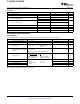
TERMINAL FUNCTIONS (FOR ZQS PACKAGE)
TERMINAL
I/O DESCRIPTION
NAME NO.
A0 D5
Register select. A0 − A2 are used during read and write operations to select the ACE register
A1 E5 I
to read from or write to. See Table 1 for register addresses, and see the ADS description.
A2 E4
Chip select. When CS2 is low, the ACE is selected. When CS2 is high, the ACE remains
CS2 D1 I
inactive.
Clear to send. CTS is a modem status signal. Its condition can be checked by reading bit 4
( CTS) of the modem status register. Bit 0 ( Δ CTS) of the modem status register indicates that
CTS C4 I CTS has changed states since the last read from the modem status register. If the modem
status interrupt is enabled when CTS changes levels and the auto- CTS mode is not enabled,
an interrupt is generated. CTS is also used in the auto-CTS mode to control the transmitter.
D0 A4
D1 B4
D2 A3
D3 B3 Data bus. Eight data lines with 3-state outputs provide a bidirectional path for data, control,
I/O
D4 A2 and status information between the ACE and the CPU.
D5 A1
D6 C3
D7 B1
Interrupt. When active (high), INTRPT informs the CPU that the ACE has an interrupt to be
serviced. Four conditions that cause an interrupt to be issued are: a receiver error, received
INTRPT D4 O data that is available or timed out (FIFO mode only), an empty transmitter holding register, or
an enabled modem status interrupt. INTRPT is reset (deactivated) either when the interrupt
is serviced or as a result of a master reset.
Master reset. When active (high), MR clears most ACE registers and sets the levels of
MR B5
various output signals (see Table 2).
Read input. When RD1 is active (low) while the ACE is selected, the CPU is allowed to read
RD1 D3 I
status information or data from a selected ACE register.
Request to send. When active, RTS informs the modem or data set that the ACE is ready to
receive data. RTS is set to the active level by setting the RTS modem control register bit and
RTS C5 O is set to the inactive (high) level either as a result of a master reset or during loop mode
operations or by clearing bit 1 ( RTS) of the MCR. In the auto- RTS mode, RTS is set to the
inactive level by the receiver threshold control logic.
SIN C1 I Serial data input. SIN is serial data input from a connected communications device.
Serial data output. SOUT is composite serial data output to a connected communication
SOUT C2 O
device. SOUT is set to the marking (high) level as a result of master reset.
V
CC
A5 2.25-V to 5.5-V power supply voltage
V
SS
E3 Supply common, ground
Write input. When WR1 is active (low) and while the ACE is selected, the CPU is allowed to
WR1 D2 I
write control words or data into a selected ACE register.
XIN E1 External clock. XIN and XOUT connect the ACE to the main timing reference (clock or
I/O
XOUT E2 crystal).
12 Submit Documentation Feedback Copyright © 2004 – 2008, Texas Instruments Incorporated
Product Folder Link(s): TL16C550D TL16C550DI