
Datasheet


SLLS037C − MARCH 1988 − REVISED JANUARY 2006
5
POST OFFICE BOX 655303 • DALLAS, TEXAS 75265
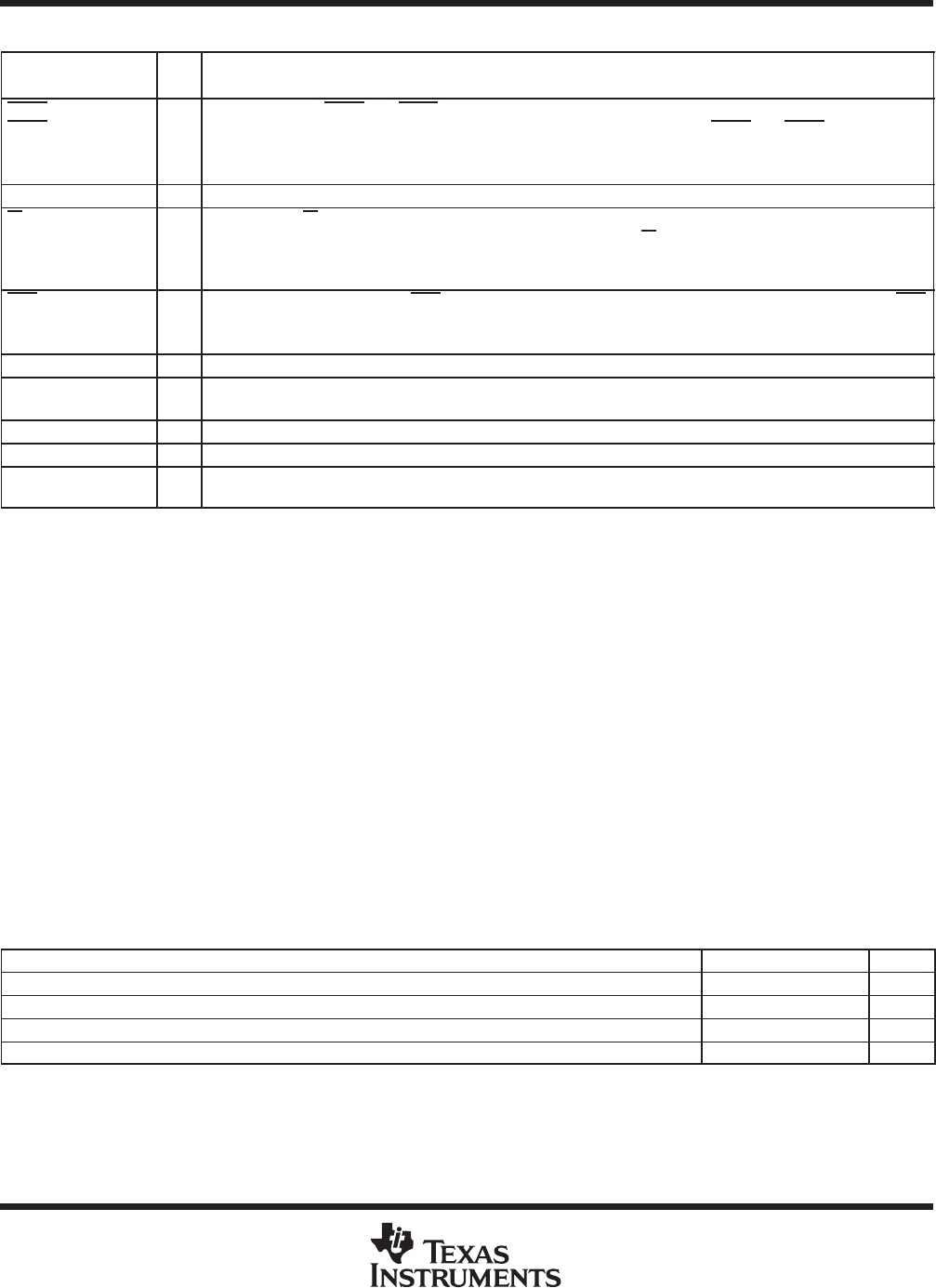
Terminal Functions (continued)
TERMINAL
I/O
DESCRIPTION
NAME NO.
†
I/O
DESCRIPTION
OUT1
OUT2
38
35
O
Outputs 1 and 2. OUT1 and OUT2 are user-designated output terminals that are set to their active states by
setting their respective modem control register bits (OUT1 and OUT2) high. OUT1
and OUT2 are set to their
inactive (high) states as a result of master reset or during loop mode operations or by clearing bit 2 (OUT1) or
bit 3 (OUT2) of the MCR.
RCLK 10 I Receiver clock. RCLK is the 16× baud rate clock for the receiver section of the ACE.
RI
43 I
Ring indicator. RI is a modem status signal. Its condition can be checked by reading bit 6 (RI) of the modem status
register. Bit 2 (TERI) of the modem status register indicates that the RI
input has transitioned from a low to a high
state since the last read from the modem status register. If the modem status interrupt is enabled when this
transition occurs, an interrupt is generated.
RTS
36 O
Request to send. When active, RTS informs the modem or data set that the ACE is ready to transmit data. RTS
is set to its active state by setting the RTS modem control register bit and is set to its inactive (high) state either
as a result of a master reset or during loop mode operations or by clearing bit 1 (RTS) of the MCR.
SIN 11 I Serial input. SIN is the serial data input from a connected communications device.
SOUT 13 O Serial output. SOUT is the composite serial data output to a connected communication device. SOUT is set to
the marking (set) state as a result of MR.
V
CC
44 5-V supply voltage
V
SS
22 Supply common
XTAL1
XTAL2
18
19
I/O External clock. XTAL1 and XTAL2 connect the ACE to the main timing reference (clock or crystal).
†
Terminal numbers shown are for the FN package.
absolute maximum ratings over free-air temperature range (unless otherwise noted)
†
Supply voltage range, V
CC
(see Note 1) −0.5 V to 7 V. . . . . . . . . . . . . . . . . . . . . . . . . . . . . . . . . . . . . . . . . . . . . .
Input voltage range at any input, V
I
−0.5 V to 7 V. . . . . . . . . . . . . . . . . . . . . . . . . . . . . . . . . . . . . . . . . . . . . . . . . .
Output voltage range, V
O
−0.5 V to 7 V. . . . . . . . . . . . . . . . . . . . . . . . . . . . . . . . . . . . . . . . . . . . . . . . . . . . . . . . . . .
Continuous total power dissipation at (or below) 70°C free-air temperature: FN package 1100 mW. . . . . . .
N package
‡
800 mW. . . . . . . .
Operating free-air temperature range, T
A
0°C to 70°C. . . . . . . . . . . . . . . . . . . . . . . . . . . . . . . . . . . . . . . . . . . . . .
Storage temperature range, T
stg
−65°C to 150°C. . . . . . . . . . . . . . . . . . . . . . . . . . . . . . . . . . . . . . . . . . . . . . . . . .
Case temperature for 10 seconds, T
C
: FN package 260°C. . . . . . . . . . . . . . . . . . . . . . . . . . . . . . . . . . . . . . . . . .
Lead temperature 1,6 mm (1/16 inch) from case for 10 seconds: N package
‡
260°C. . . . . . . . . . . . . . . . . . . .
†
Stresses beyond those listed under “absolute maximum ratings” may cause permanent damage to the device. These are stress ratings only and
functional operation of the device at these or any other conditions beyond those indicated under “recommended operating conditions” is not
implied. Exposure to absolute-maximum-rated conditions for extended periods may affect device reliability.
‡
The N package in Not Recommended for New Designs.
NOTE 1: All voltage values are with respect to V
SS
.
recommended operating conditions
MIN NOM MAX UNIT
Supply voltage, V
CC
4.75 5 5.25 V
High-level input voltage, V
IH
2 V
CC
V
Low-level input voltage, V
IL
−0.5 0.8 V
Operating free-air temperature, T
A
0 70 °C