
Datasheet


SLOS078J − NOVEMBER 1978 − REVISED SEPTEMBER 2004
5
POST OFFICE BOX 655303 • DALLAS, TEXAS 75265
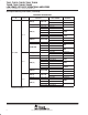
absolute maximum ratings over operating free-air temperature range (unless otherwise noted)
†
TL06_C
TL06_AC
TL06_BC
TL06_I TL06_M UNIT
Supply voltage, V
CC+
(see Note 1) 18 18 18 V
Supply voltage, V
CC−
(see Note 1) −18 −18 −18 V
Differential input voltage, V
ID
(see Note 2) ±30 ±30 ±30 V
Input voltage, V
I
(see Notes 1 and 3) ±15 ±15 ±15 V
Duration of output short circuit (see Note 4) Unlimited Unlimited Unlimited
D (8-pin) package 97 97
D (14-pin) package 86 86
N package 80 80
NS package 76 76
Package thermal impedance, θ
JA
(see Notes 5 and 6)
P package 85 85
°C/W
Package thermal impedance,
JA
(see Notes 5 and 6)
PS package 95 95
C/W
PW (8-pin) package 149 149
PW (14-pin)
package
113 113
FK package 5.61
Package thermal impedance, θ
JC
(see Notes 7 and 8)
J package 15.05
°C/W
Package thermal impedance, θ
JC
(see Notes 7 and 8)
JG package 14.5
°C/W
W package 14.65
Operating virtual junction temperature, T
J
150 150 150 °C
Case temperature for 60 seconds FK package 260 °C
Lead temperature 1,6 mm (1/16 inch) from case for 60
J, JG, U, or
300
°C
Lead temperature 1,6 mm (1/16 inch) from case for 60
seconds
J, JG, U, or
W package
300 °C
Lead temperature 1,6 mm (1/6 inch) from case for 10
D, N, NS, P, PS,
260
260
°C
Lead temperature 1,6 mm (1/6 inch) from case for 10
seconds
D, N, NS, P, PS,
or PW package
260
260
°
C
Storage temperature range, T
stg
−65 to 150 −65 to 150 −65 to 150 °C
†
Stresses beyond those listed under “absolute maximum ratings” may cause permanent damage to the device. These are stress ratings only, and
functional operation of the device at these or any other conditions beyond those indicated under “recommended operating conditions” is not
implied. Exposure to absolute-maximum-rated conditions for extended periods may affect device reliability.
NOTES: 1. All voltage values except differential voltages are with respect to the midpoint between V
CC+
and V
CC−
.
2. Differential voltages are at IN+ with respect to IN−.
3. The magnitude of the input voltage should never exceed the magnitude of the supply voltage or 15 V, whichever is less.
4. The output may be shorted to ground or to either supply. Temperature and/or supply voltages must be limited to ensure that the
dissipation rating is not exceeded.
5. Maximum power dissipation is a function of T
J
(max), θ
JA
, and T
A
. The maximum allowable power dissipation at any allowable
ambient temperature is P
D
= (T
J
(max) − T
A
)/θ
JA
. Operating at the absolute maximum T
J
of 150°C can affect reliability.
6. The package thermal impedance is calculated in accordance with JESD 51-7.
7. Maximum power dissipation is a function of T
J
(max), θ
JC
, and T
C
. The maximum allowable power dissipation at any allowable case
temperature is P
D
= (T
J
(max) − T
C
)/θ
JC
. Operating at the absolute maximum T
J
of 150°C can affect reliability.
8. The package thermal impedance is calculated in accordance with MIL-STD-883.