
Datasheet


NC
VCC+
IN1í
IN1+
VCCí
NC
OUT
NC
RG
RIN
RF
GND
VIN
VS-GND
VS+
GND
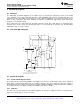
Run the input traces as far
away from the supply lines
as possible
Only needed for
dual-supply
operation
Place components close to
device and to each other to
reduce parasitic errors
Use low-ESR, ceramic
bypass capacitor
(or GND for single supply) Ground (GND) plane on another layerVOUT
+
RIN
RG
RF
VOUT
VIN
TL061
,
TL061A
,
TL061B
TL062
,
TL062A
,
TL062B
,
TL064
,
TL064A
,
TL064B
SLOS078L –NOVEMBER 1978–REVISED MAY 2015
www.ti.com
11 Layout
11.1 Layout Guidelines
For best operational performance of the device, use good PCB layout practices, including:
• Noise can propagate into analog circuitry through the power pins of the circuit as a whole, as well as the
operational amplifier. Bypass capacitors are used to reduce the coupled noise by providing low impedance
power sources local to the analog circuitry.
– Connect low-ESR, 0.1-μF ceramic bypass capacitors between each supply pin and ground, placed as
close to the device as possible. A single bypass capacitor from V+ to ground is applicable for single
supply applications.
• Separate grounding for analog and digital portions of circuitry is one of the simplest and most-effective
methods of noise suppression. One or more layers on multilayer PCBs are usually devoted to ground planes.
A ground plane helps distribute heat and reduces EMI noise pickup. Make sure to physically separate digital
and analog grounds, paying attention to the flow of the ground current. For more detailed information, refer to
Circuit Board Layout Techniques, (SLOA089).
• To reduce parasitic coupling, run the input traces as far away from the supply or output traces as possible. If
it is not possible to keep them separate, it is much better to cross the sensitive trace perpendicular as
opposed to in parallel with the noisy trace.
• Place the external components as close to the device as possible. Keeping RF and RG close to the inverting
input minimizes parasitic capacitance, as shown in Layout Examples.
• Keep the length of input traces as short as possible. Always remember that the input traces are the most
sensitive part of the circuit.
• Consider a driven, low-impedance guard ring around the critical traces. A guard ring can significantly reduce
leakage currents from nearby traces that are at different potentials.
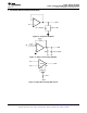
11.2 Layout Examples
Figure 30. Operational Amplifier Schematic for Noninverting Configuration
Figure 31. Operational Amplifier Board Layout for Noninverting Configuration
20 Submit Documentation Feedback Copyright © 1978–2015, Texas Instruments Incorporated
Product Folder Links: TL061 TL061A TL061B TL062 TL062A TL062B TL064 TL064A TL064B