
Datasheet


TL05x, TL05xA
ENHANCED-JFET LOW-OFFSET
OPERATIONAL AMPLIFIERS
SLOS178A – FEBRUARY 1997 - REVISED FEBRUARY 2003
11
POST OFFICE BOX 655303 • DALLAS, TEXAS 75265
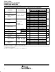
TL052I and TL052AI electrical characteristics at specified free-air temperature
TL052I, TL052AI
PARAMETER TEST CONDITIONS
T
A
†
V
CC±
= ±5 V V
CC±
= ±15 V
UNIT
A
MIN TYP MAX MIN TYP MAX
TL052I
25°C 0.73 3.5 0.65 1.5
V
IO
In
p
ut offset voltage
TL052I
Full range 5.3 3.3
mV
V
IO
Input
offset
voltage
V0
TL052AI
25°C 0.51 2.8 0.4 0.8
mV
V
O
=
0
,
V
IC
=
0,
TL052AI
Full range 4.6 2.6
Ttffiit
‡
V
IC
=
0
,
R
S
= 50 Ω
TL052I
25°C to
85°C
7 6
µV/°C
V
IO
T
empera
t
ure coe
ffi
c
i
en
t
‡
TL052AI
25°C to
85°C
6 6 25
µ
V/°C
Input offset-voltage
long-term drift
§
V
O
= 0,
R
S
= 50 Ω
V
IC
= 0, 25°C 0.04 0.04 µV/mo
I
IO
In
p
ut offset current
V
O
= 0, V
IC
= 0,
25°C 4 100 5 100 pA
I
IO
Input
offset
current
O
,
See Figure 5
IC
,
85°C 0.06 10 0.07 10 nA
I
IB
In
p
ut bias current
V
O
= 0, V
IC
= 0,
25°C 20 200 30 200 pA
I
IB
Input
bias
current
O
,
See Figure 5
IC
,
85°C 0.6 20 0.7 20 nA
V
ICR
Common-mode input
25°C
–1
to
4
–2.3
to
5.6
–11
to
11
–12.3
to
15.6
V
V
ICR
voltage range
Full range
–1
to
4
–11
to
11
V
R
L
=10kΩ
25°C 3 4.2 13 13.9
V
OM
Maximum positive peak
R
L
=
10
kΩ
Full range 3 13
V
V
OM+
output voltage swing
R
L
=2kΩ
25°C 2.5 3.8 11.5 12.7
V
R
L
=
2
kΩ
Full range 2.5 11.5
R
L
=10kΩ
25°C –2.5 –3.5 –12 –13.2
V
OM
Maximum ne
g
ative peak
R
L
=
10
kΩ
Full range –2.5 –12
V
V
OM–
g
output voltage swing
R
L
=2kΩ
25°C –2.3 –3.2 –11 –12
V
R
L
=
2
kΩ
Full range –2.3 –11
L i l diff ti l
25°C 25 59 50 105
A
VD
Large-signal differential
voltage am
p
lification
¶
R
L
= 2 kΩ
–40°C 30 74 60 145
V/mV
voltage
am lification
¶
85°C 20 43 30 76
r
i
Input resistance 25°C 10
12
10
12
Ω
c
i
Input capacitance 25°C 10 12 pF
Common mode
V V min
25°C 65 85 75 93
CMRR
C
ommon-mo
d
e
rejection ratio
V
IC
=
V
ICR
m
i
n,
V
O
=
0,
R
S
= 50 Ω
–40°C 65 83 75 90
dB
rejection
ratio
V
O
=
0
,
85°C 65 84 75 93
†
Full range is –40°C to 85°C.
‡
This parameter is tested on a sample basis. For other test requirements, please contact the factory. This statement has no bearing on testing
or nontesting of other parameters
§
Typical values are based on the input offset-voltage shift observed through 168 hours of operating life test at T
A
= 150°C, extrapolated to
T
A
= 25°C using the Arrhenius equation, and assuming an activation energy of 0.96 eV.
¶
At V
CC±
= ±5 V, V
O
= ±2.3 V; at V
CC±
= ±15 V, V
O
= ±10 V.