
Datasheet


TL05x, TL05xA
ENHANCED-JFET LOW-OFFSET
OPERATIONAL AMPLIFIERS
SLOS178A – FEBRUARY 1997 - REVISED FEBRUARY 2003
18
POST OFFICE BOX 655303 • DALLAS, TEXAS 75265
TYPICAL CHARACTERISTICS
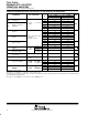
Table of Graphs
FIGURE
V
IO
Input offset voltage Distribution 6–11
V
IO
Temperature coefficient of input offset voltage Distribution 12, 13, 14
I
IB
Input bias current
vs Common-mode input voltage
vs Free-air temperature
15
16
I
IO
Input offset current vs Free-air temperature 16
V
IC
Common-mode input voltage range limits
vs Supply voltage
vs Free-air temperature
17
18
V
O
Output voltage vs Differential input voltage 19, 20
V
OM
Maximum peak output voltage
vs Supply voltage
vs Output current
vs Free-air temperature
21
25, 26
27, 28
V
O(PP)
Maximum peak-to-peak output voltage vs Frequency 22, 23, 24
A
VD
Large-signal differential voltage amplification
vs Load resistance
vs Frequency
vs Free-air temperature
29
30
31, 32, 33
CMRR Common-mode rejection ratio
vs Frequency
vs Free-air temperature
34, 35
36
z
o
Output impedance vs Frequency 37
k
SVR
Supply-voltage rejection ratio vs Free-air temperature 38
I
OS
Short-circuit output current
vs Supply voltage
vs Time
vs Free-air temperature
39
40
41
I
CC
Supply current
vs Supply voltage
vs Free-air temperature
42, 43, 44
45, 46, 47
SR Slew rate
vs Load resistance
vs Free-air temperature
48–53
54–59
Overshoot factor vs Load capacitance 60
V
n
Equivalent input noise voltage vs Frequency 61, 62
THD Total harmonic distortion vs Frequency 63
B
1
Unity-gain bandwidth
vs Supply voltage
vs Free-air temperature
64, 65, 66
67, 68, 69
φ
m
Phase margin
vs Supply voltage
vs Load capacitance
vs Free-air temperature
70, 71, 72
73, 74, 75
76, 77, 78
Phase shift vs Frequency 30
Voltage-follower small-signal pulse response vs Time 79
Voltage-follower large-signal pulse response vs Time 80