
Datasheet


TL05x, TL05xA
ENHANCED-JFET LOW-OFFSET
OPERATIONAL AMPLIFIERS
SLOS178A – FEBRUARY 1997 - REVISED FEBRUARY 2003
44
POST OFFICE BOX 655303 • DALLAS, TEXAS 75265
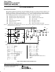
APPLICATION INFORMATION
high input impedance log amplifier
The low input offset voltage and high input impedance of the TL05xA creates a precision log amplifier (see
Figure 87). IC1 is a 2.5-V, low-current precision, shunt regulator. Transistors Q1 and Q2 must be a closely
matched npn pair. For best performance over temperature, R4 should be a metal-film resistor with a low
temperature coefficient.
In this circuit, U1A serves as a high-impedance unity-gain buffer. Amplifier U1B converts the input voltage to
a current through R1 and Q1. Amplifier U1C, IC1, and R4 form a 1-µA temperature-stable current source that
sets the base-emitter voltage of Q2. U1D amplifies the difference between the base-emitter voltage of Q1 and
Q2 (see Figure 88). The output voltage is given by the following equation:
V
O
–
1
R6
R5
kT
q
In
V
I
R1 1 10
–6
where k 1.38 10
–23
,q 1.602 10
–19
,
and T is Kelvin temperature
_
+
_
+
U1A
_
+
U1B
_
+
U1C
U1D
V
I
R1
10 kΩ
Q1 Q2
2N2484
R2
15 V
10 kΩ
2.5 MΩ
R4
150 pF
C1
IC1
270 kΩ
R3
–15V
R5
10 kΩ
R6
10 kΩ
V
O
(see equation above)
NOTE A: U1A through U1D = TL05xA. IC1 = LM385, LT1004, or LT1009 voltage reference
Figure 87. Log Amplifier
0123456
– Differential Voltage Amplification – dB
f – Frequency – Hz
78910
–0.4
–0.35
–0.3
–0.25
–0.2
–0.15
–0.1
A
VD
Figure 88. Output Voltage vs Input Voltage for Log Amplifier