
Datasheet


TL05x, TL05xA
ENHANCED-JFET LOW-OFFSET
OPERATIONAL AMPLIFIERS
SLOS178A – FEBRUARY 1997 - REVISED FEBRUARY 2003
13
POST OFFICE BOX 655303 • DALLAS, TEXAS 75265
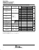
TL054C and TL054AC electrical characteristics at specified free-air temperature
†
TL054C, TL054AC
PARAMETER TEST CONDITIONS
T
A
†
V
CC±
= ±5 V V
CC±
= ±15 V
UNIT
MIN TYP MAX MIN TYP MAX
TL054C
25°C 0.64 5.5 0.56 4
V
IO
In
p
ut offset voltage
TL054C
Full range 7.7 6.2
mV
V
IO
Input
offset
voltage
TL054AC
25°C 0.57 3.5 0.5 1.5
mV
V
O
=0
TL054AC
Full range 5.7 3.7
Temperature coefficient
V
O
=
0
,
V
IC
= 0,
R
S
= 50 Ω
TL054C
25°C to
70°C
25 23
µV/
°
C
V
IO
of input offset voltage
R
S
50
Ω
TL054AC
25°C to
70°C
24 23
µ
V/°C
Input offset-voltage
long-term drift
‡
25°C 0.04 0.04 µV/mo
I
IO
In
p
ut offset current
V
O
= 0, V
IC
= 0,
25°C 4 100 5 100 pA
I
IO
Input
offset
current
OIC
See Figure 5
70°C 0.02 1 0.025 1 nA
I
IB
In
p
ut bias current
V
O
= 0, V
IC
= 0,
25°C 20 200 30 200 pA
I
IB
Input
bias
current
OIC
See Figure 5
70°C 0.15 4 0.2 4 nA
V
ICR
Common-mode input
25°C
–1
to
4
–2.3
to
5.6
–11
to
11
–12.3
to
15.6
V
V
ICR
voltage range
Full range
–1
to
4
–11
to
11
V
R
L
=10kΩ
25°C 3 4.2 13 13.9
V
OM
Maximum positive peak
R
L
=
10
kΩ
Full range 3 13
V
V
OM+
output voltage swing
R
L
=2kΩ
25°C 2.5 3.8 11.5 12.7
V
R
L
=
2
kΩ
Full range 2.5 11.5
R
L
=10kΩ
25°C –2.5 –3.5 –12 –13.2
V
OM
Maximum negative peak
R
L
=
10
kΩ
Full range –2.5 –12
V
V
OM–
g
output voltage swing
R
L
=2kΩ
25°C –2.3 –3.2 –11 –12
V
R
L
=
2
kΩ
Full range –2.3 –11
L i l diff ti l
25°C 25 72 50 133
A
VD
L
arge-s
i
gna
l
diff
eren
ti
a
l
voltage am
p
lification
§
R
L
= 2 kΩ 0°C 30 88 60 173 V/mV
voltage
am lification
§
70°C 20 57 30 85
r
i
Input resistance 25°C
10
12
10
12
Ω
c
i
Input capacitance 25°C 10 12 pF
Common mode
V V min
25°C 65 84 75 92
CMRR
C
ommon-mo
d
e
rejection ratio
V
IC
=
V
ICR
m
i
n,
V
O
=0 R
S
=50Ω
0°C 65 84 75 92 dB
rejection
ratio
V
O
=
0
,
R
S
=
50
Ω
70°C 65 84 75 93
Supply voltage rejection
V ±5Vto±15 V
25°C 75 99 75 99
k
SVR
S
upp
l
y-vo
lt
age re
j
ec
ti
on
ratio (∆V
CC±
/∆V
IO
)
V
CC±
=
±5
V
t
o
±15
V
,
V
O
=0 R
S
=50Ω
0°C 75 99 75 99 dB
ratio
(∆V
CC±
/∆V
IO
)
V
O
=
0
,
R
S
=
50
Ω
70°C 75 99 75 99
Supply current
25°C 8.1 11.2 8.4 11.2
I
CC
S
upp
l
y curren
t
(four am
p
lifiers)
V
O
= 0, No load 0°C 8.2 12.8 8.5 12.8 mA
(four
am lifiers)
70°C 7.9 11.2 8.2 11.2
V
O1
/V
O2
Crosstalk attenuation A
VD
= 100 25°C 120 120 dB
†
Full range is 0°C to 70°C.
‡
Typical values are based on the input offset-voltage shift observed through 168 hours of operating life test at T
A
= 150°C, extrapolated to
T
A
= 25°C using the Arrhenius equation, and assuming an activation energy of 0.96 eV.
§
For V
CC±
= ±5 V, V
O
= ±2.3 V, at V
CC±
= ±15 V, V
O
= ±10 V.B