
Datasheet


THS8200
www.ti.com
SLES032D –JUNE 2002–REVISED JUNE 2013
7 Electrical Characteristics
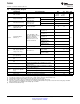
7.1 Absolute Maximum Ratings
over operating temperature range (unless otherwise noted)
(1)
AV
DD
to AV
SS
, VDD_IO to GND_IO −0.5 V to 4.5 V
Supply voltage range
DV
DD
to DV
SS
, VDD_DLL to DVSS −0.5 V to 2.5 V
Digital input voltage range to DV
SS
−0.5 V to (VDD_IO + 0.5 V)
T
A
Operating free-air temperature range 0°C to 70°C
T
stg
Storage temperature range −55°C to 150°C
(1) Stresses beyond those listed under absolute maximum ratings may cause permanent damage to the device. These are stress ratings
only, and functional operation of the device at these or any other conditions beyond those indicated under recommended operating
conditions is not implied. Exposure to absolute-maximum-rated conditions for extended periods may affect device reliability.
7.2 Recommended Operating Conditions
over operating free-air temperature range, T
A
MIN NOM MAX UNIT
POWER SUPPLY
AV
DD
3 3.3 3.6
Supply voltage DV
DD
, VDD_DLL 1.65 1.8 2 V
VDD_IO 1.65 1.8/3.3 3.6
DIGITAL AND REFERENCE INPUTS
VDD_IO = 1.8 V 0.95 VDD_IO
V
IH
High-level input voltage V
VDD_IO = 3.3 V 2.3 VDD_IO
VDD_IO = 1.8 V DV
SS
0.4
V
IL
Low-level input voltage V
VDD_IO = 3.3 V DV
SS
1.15
f
clk
Clock frequency 10 205 MHz
t
w(CLKH)
Pulse duration, clock high 40% 60%
t
w(CLKL)
Pulse duration, clock low 40% 60%
V
OC
= 700 mV 2.99
R
FS
FSADJ resistor kΩ
V
OC
= 1 V 2.08
Copyright © 2002–2013, Texas Instruments Incorporated Electrical Characteristics 83
Submit Documentation Feedback
Product Folder Links: THS8200