
Datasheet


G0/Y0
GY[9:0]/[9:2]
CLKIN
G1/Y1 G2/Y2 G3/Y3 G4/Y4 G5/Y5 G6/Y6 G7/Y7
B0/Cb0
BCb[9:0]/[9:2]
B1/Cb1 B2/Cb2 B3/Cb3 B4/Cb4 B5/Cb5 B6/Cb6 B7/Cb7
R0/Cr0
RCr[9:0]/[9:2]
R1/Cr1 R2/Cr2 R3/Cr3 R4/Cr4 R5/Cr5 R6/Cr6 R7/Cr7
THS8200
SLES032D –JUNE 2002–REVISED JUNE 2013
www.ti.com
Furthermore, Table 4-1 shows for which modes presets are defined. When in a preset video mode, the
line-type/breakpoint-pairs that define the frame format (see Section 4.7) are preprogrammed. Therefore
the user does not need to define the table with line type/breakpoint settings, nor does the field and frame
size need to be programmed. However, when in preset mode, the horizontal parameters (all dtg1_spec_x
registers for the line types used by the preset setting, and dtg1_total_pixels registers) still need to be
programmed. Presets are available for most popular DTV video formats. Alternatively, generic modes for
SDTV, HDTV or VESA can be selected, which allow full programmability of the field/frame sizes and DTG
parameters.
Note from the table that:
• If embedded timing is used, the device is always in slave mode, because the data stream supplied to
THS8200 contains the video timing information.
• Master operation is only supported for PC graphics (VESA) formats.
• In HDTV modes with embedded timing, data is supplied to the device over a 20-bit interface, as
defined in SMPTE274/296M.
• In SDTV modes with embedded timing, data is supplied to the device over a 10-bit interface. When the
video format is interlaced, this interface is known as ITU-R.BT656 (525I, 625I). When the video format
is progressive, only 525P is supported with embedded timing. The 625P interface can be supported
with dedicated timing, using the SDTV generic mode.
• In generic modes with dedicated timing, both 20 bits (4:2:2) and 30 bits (4:4:4) are supported.
• In PC graphics modes (VESA generic), input data is either over the 30-bit interface or over the 16-/15-
bit interface and always has dedicated timing. Note that the 16-bit interface is not equivalent to a 2x8-
bit version of the 20-bit interface; see Section 4.2 for details.
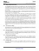
4.2 Input Interface Formats
The following figures define the input video format for each input mode, as selected by the
data_dman_cntl register setting. Video data is always clocked in at the rising edge of CLKIN.
NOTE
For 8-bit operation with 10-bit input buses, connect only the 8 MSBs of each input bus used,
and tie the 2 LSBs to ground.
• 30-bit YCbCr/RGB 4:4:4
Figure 4-1. 24-/30-Bit RGB or YCbCr Data Format
• 20-bit YCbCr 4:2:2
CLKIN is equal to the 1x pixel clock. The pixel clock equals the rate of the Y input and is 2x the rate of
the 2 other channels in this input format where Cb and Cr are multiplexed onto the same input bus.
18 Detailed Functional Description Copyright © 2002–2013, Texas Instruments Incorporated
Submit Documentation Feedback
Product Folder Links: THS8200