
Datasheet


www.ti.com
Offset Voltage
Noise Calculations and Noise Figure
_
+
R
F
R
S
R
G
e
Rg
e
Rf
e
Rs
e
n
IN+
Noiseless
IN–
e
ni
e
no
S0277-01
THS6022
SLOS225D – SEPTEMBER 1998 – REVISED JULY 2007
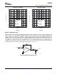
The output offset voltage, (V
OO
) is the sum of the input offset voltage (V
IO
) and both input bias currents (I
IB
)
times the corresponding gains. The following schematic and formula can be used to calculate the output offset
voltage:
Figure 50. Output Offset Voltage Model
Noise can cause errors on very small signals. This is especially true for amplifying small signals. The noise
model for current-feedback amplifiers (CFB) is the same as for voltage-feedback amplifiers (VFB). The only
difference between the two is that the CFB amplifiers generally specify different current noise parameters for
each input, whereas VFB amplifiers usually only specify one noise-current parameter. The noise model is shown
in Figure 51 . This model includes all of the noise sources as follows:
• e
n
= Amplifier internal voltage noise (nV/ √ Hz)
• IN+ = Noninverting current noise (pA/ √ Hz)
• IN– = Inverting current noise (pA/ √ Hz)
• e
Rx
= Thermal voltage noise associated with each resistor (e
Rx
= 4 kTR
x
)
Figure 51. Noise Model
24
Submit Documentation Feedback