
Datasheet


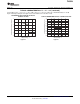


Output Measured
Here With High
Impedance
Differential Probe
THS4509
CM
V
IN
R
F
R
F
R
G
R
G
R
IT
R
IT
From
50 Ω
Source V
S+
V
S−
49.9 Ω
49.9 Ω
100 Ω
0.22 µF
49.9 Ω
0.22 µF
Open
THS 4509
CM
From
50 Ω
Source
V
IN
0.22 µF
49.9 Ω
V
OUT
Open
To 50 Ω
Test
Equipment
R
G
R
IT
R
G
R
IT
R
F
V
S+
V
S−
R
O
R
O
R
OT
0.22 µF
1:1
R
F
THS4509
SLOS454H –JANUARY 2005–REVISED NOVEMBER 2009
www.ti.com
TEST CIRCUITS
The THS4509 is tested with the following test circuits
built on the evaluation module (EVM). For simplicity,
power-supply decoupling is not shown—see the
Layout Recommendations in the Applications section
for recommendations. Depending on the test
conditions, component values are changed per the
following tables, or as otherwise noted. The signal
generators used are ac-coupled, 50-Ω sources, and a
0.22-μF capacitor and 49.9-Ω resistor to ground are
inserted across R
IT
on the alternate input to balance
Figure 76. Frequency Response Test Circuit
the circuit. A split power supply is used to ease the
interface to common test equipment, but the amplifier
A network analyzer is used as the signal source and
can be operated single-supply as described in the
as the measurement device. The output impedance
Applications section with no impact on performance.
of the network analyzer is 50 Ω. R
IT
and R
G
are
chosen to impedance match to 50 Ω, and to maintain
Table 1. Gain Component Values
the proper gain. To balance the amplifier, a 0.22-μF
GAIN R
F
R
G
R
IT
capacitor and 49.9-Ω resistor to ground are inserted
across R
IT
on the alternate input.
6 dB 348 Ω 165 Ω 61.9 Ω
10 dB 348 Ω 100 Ω 69.8 Ω
The output is probed using a high-impedance
14 dB 348 Ω 56.2 Ω 88.7 Ω
differential probe across the 100-Ω resistor. The gain
is referred to the amplifier output by adding back the
20 dB 348 Ω 16.5 Ω 287 Ω
6-dB loss due to the voltage divider on the output.
Note the gain setting includes 50-Ω source
impedance. Components are chosen to achieve
Distortion and 1-dB Compression
gain and 50-Ω input termination.
The circuit shown in Figure 77 is used to measure
harmonic distortion, intermodulation distortion, and
Table 2. Load Component Values
1-db compression point of the amplifier.
R
L
R
O
R
OT
ATTEN.
100 Ω 25 Ω Open 6 dB
200 Ω 86.6 Ω 69.8 Ω 16.8 dB
499 Ω 237 Ω 56.2 Ω 25.5 dB
1k Ω 487 Ω 52.3 Ω 31.8 dB
Note the total load includes 50-Ω termination by
the test equipment. Components are chosen to
achieve load and 50-Ω line termination through a
1:1 transformer.
Due to the voltage divider on the output formed by
Figure 77. Distortion Test Circuit
the load component values, the amplifier output is
attenuated. The column Atten in Table 2 shows the
attenuation expected from the resistor divider. When
using a transformer at the output as shown in
Figure 77, the signal will see slightly more loss, and
these numbers will be approximate.
Frequency Response
The circuit shown in Figure 76 is used to measure the
frequency response of the circuit.
24 Submit Documentation Feedback Copyright © 2005–2009, Texas Instruments Incorporated
Product Folder Link(s): THS4509