
Datasheet


SETTING THE OUTPUT COMMON-MODE
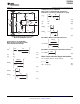
V
OCM
=2.5V
5V
V
S
R
S
R
G1
R
G2
R
F1
R
F2
+
R
T
+
R
S
2.5-VDC
2.5-VDC
DCCurrentPathtoGround
DCCurrentPathtoGround
I
2
=
V
OCM
R
F2 G2
+R
I
1
=
V
OCM
R
F1 G1 S T
+R +R ||R
-
-
R =50kW
R =50kW
V
S+
V
S-
V
OCM
I
IN
I
IN
=
2V V V- -
OCM S
S+
-
R
THS4504
THS4505
SLOS363D – AUGUST 2002 – REVISED MAY 2008 .........................................................................................................................................................
www.ti.com
Often times, filters like these are used to eliminate for the sole purpose of filtering any high frequency
broadband noise and out-of-band distortion products noise that could couple into the signal path through
in signal acquisition systems. It should be noted that the V
OCM
circuitry. A 0.1- µ F or 1- µ F capacitance is a
the increased load placed on the output of the reasonable value for eliminating a great deal of
amplifier by the second low-pass filter has a broadband interference, but additional, tuned
detrimental effect on the distortion performance. The decoupling capacitors should be considered if a
preferred method of filtering is using the feedback specific source of electromagnetic or radio frequency
network, as the typically smaller capacitances interference is present elsewhere in the system.
required at these points in the circuit do not load the Information on the ac performance (bandwidth, slew
amplifier nearly as heavily in the pass-band. rate) of the V
OCM
circuitry is included in the
specification table and graph section.
Since the V
OCM
pin provides the ability to set an
VOLTAGE WITH THE V
OCM
INPUT
output common-mode voltage, the ability for
increased power dissipation exists. While this does
The output common-mode voltage pin provides a
not pose a performance problem for the amplifier, it
critical function to the fully differential amplifier; it
can cause additional power dissipation of which the
accepts an input voltage and reproduces that input
system designer should be aware. The circuit shown
voltage as the output common-mode voltage. In other
in Figure 84 demonstrates an example of this
words, the V
OCM
input provides the ability to level-shift
phenomenon. For a device operating on a single 5-V
the outputs to any voltage inside the output voltage
supply with an input signal referenced around ground
swing of the amplifier.
and an output common-mode voltage of 2.5 V, a dc
A description of the input circuitry of the V
OCM
pin is
potential exists between the outputs and the inputs of
shown below to facilitate an easier understanding of
the device. The amplifier sources current into the
the V
OCM
interface requirements. The V
OCM
pin has
feedback network in order to provide the circuit with
two 50-k Ω resistors between the power supply rails to
the proper operating point. While there are no serious
set the default output common-mode voltage to
effects on the circuit performance, the extra power
midrail. A voltage applied to the V
OCM
pin alters the
dissipation may need to be included in the system
output common-mode voltage as long as the source
power budget.
has the ability to provide enough current to overdrive
the two 50-k Ω resistors. This phenomenon is
depicted in the V
OCM
equivalent circuit diagram.
Current drive is especially important when using the
reference voltage of an analog-to-digital converter to
drive V
OCM
. Output current drive capabilities differ
from part to part, so a voltage buffer may be
necessary in some applications.
Figure 84. Depiction of DC Power Dissipation
Figure 83. Equivalent Input Circuit for V
OCM
Caused by Output Level-Shifting in a DC-Coupled
Circuit
By design, the input signal applied to the V
OCM
pin
propagates to the outputs as a common-mode signal.
As shown in the equivalent circuit diagram, the V
OCM
input has a high impedance associated with it,
dictated by the two 50-k Ω resistors. While the high
impedance allows for relaxed drive requirements, it
also allows the pin and any associated printed-circuit
board traces to act as an antenna. For this reason, a
decoupling capacitor is recommended on this node
24 Submit Documentation Feedback Copyright © 2002 – 2008, Texas Instruments Incorporated
Product Folder Link(s): THS4504 THS4505