
Datasheet


SLOS238D − MAY 1999 − REVISED AUGUST 2008
www.ti.com
18
APPLICATION INFORMATION
OFFSET VOLTAGE
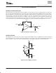
The output offset voltage, (V
OO
) is the sum of the input offset voltage (V
IO
) and both input bias currents (I
IB
) times the
corresponding gains. The following schematic and formula can be used to calculate the output offset voltage:
V
OO
+ V
IO
ǒ1 )
R
F
R
G
Ǔ" I
IB)
R
S
ǒ1 )
R
F
R
G
Ǔ" I
IB*
R
F
+
−
V
IO
+
R
G
R
S
R
F
+I
IB−
V
O
+I
IB+
−
Figure 47. Output Offset Voltage Model
OPTIMIZING UNITY GAIN RESPONSE
Internal frequency compensation of the THS405x was selected to provide very wideband performance yet still maintain
stability when operated in a noninverting unity gain configuration. When amplifiers are compensated in this manner there
is usually peaking in the closed loop response and some ringing in the step response for very fast input edges, depending
upon the application. This is because a minimum phase margin is maintained for the G=+1 configuration. For optimum
settling time and minimum ringing, a feedback resistor of 620 Ω should be used as shown in Figure 48. Additional
capacitance can also be used in parallel with the feedback resistance if even finer optimization is required.
_
+
THS405x
620 Ω
Input
Output
Figure 48. Noninverting, Unity Gain Schematic