
Datasheet


TFP410-EP
PanelBus™ DIGITAL TRANSMITTER
SGLS344A − JULY 2006 − REVISED MAY 2011
21
POST OFFICE BOX 655303 • DALLAS, TEXAS 75265
register descriptions (continued)
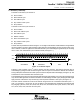
CFG Sub-Address = 0B Read Only
7
6 5 4 3 2 1 0
CFG[7:0] (D[23:16])
This read-only register contains the state of the inputs D[23:16]. These pins can be used to provide the user with
selectable configuration data through the I
2
C bus.
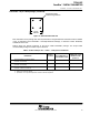
RESERVED Sub-Address = 0E−0C Read/Write Default = 0x97D0A9
7 6 5 4 3 2 1 0
RESERVED
RESERVED
RESERVED
These read/write registers have no effect on TFP410 operation.
DE_DLY Sub-Address = 32 Read/Write Default = 0x00
7 6 5 4 3 2 1 0
DE_DLY[7:0]
This read/write register defines the number of pixels after HSYNC goes active when the DE is generated and when
the DE generator is enabled. The value must be less than or equal to (2047 − DE_CNT).
DE_CTL Sub-Address = 33 Read/Write Default = 0x00
7
6 5 4 3 2 1 0
Reserved DE_GEN VS_POL HS_POL Reserved DE_DLY[8]
DE_DLY[8]: This read/write register contains the top bit of DE_DLY.
HS_POL: This read/write register sets the HSYNC polarity.
0: HSYNC is considered active low.
1: HSYNC is considered active high.
Pixel counts are reset on the HSYNC active edge.
VS_POL: This read/write register sets the VSYNC polarity.
0: VSYNC is considered active low.
1: VSYNC is considered active high.
Line counts are reset on the VSYNC active edge.
DE_GEN: This read/write register enables the internal DE generator.
0: DE generator is disabled. Signal required on DE pin.
1: DE generator is enabled. DE pin is ignored.
DE_TOP Sub-Address = 34 Read/Write Default = 0x00
7
6 5 4 3 2 1 0
DE_TOP[7:0]
This read/write register defines the number of pixels after VSYNC goes active when the DE is generated and when
the DE generator is enabled.