
Datasheet


TFP410-EP
PanelBus™ DIGITAL TRANSMITTER
SGLS344A − JULY 2006 − REVISED MAY 2011
20
POST OFFICE BOX 655303 • DALLAS, TEXAS 75265
register descriptions (continued)
HTPLG: This read only register contains the hot-plug detection input logic state.
0: Logic level detected on EDGE/HTPLG (pin 9)
1: High level detected on EDGE/HTPLG (pin 9)
RSEN: This read-only register contains the receiver sense input logic state, which is valid only for dc-coupled
systems.
0: A powered-on receiver is not detected.
1: A powered-on receiver is detected (i.e., connected to the DVI transmitter outputs).
TSEL: This read/write register contains the interrupt generation source select.
0: Interrupt bit (MDI) is generated by monitoring RSEN.
1: Interrupt bit (MDI) is generated by monitoring HTPLG.
MSEL: This read/write register contains the source select of the monitor sense output pin.
000: Disabled. MSEN output high.
001: Outputs the MDI bit (interrupt)
010: Outputs the RSEN bit (receiver detect)
011: Outputs the HTPLG bit (hot-plug detect)
VLOW: This read-only register indicates the V
REF
input level.
0: This bit is a logic level 0 if the V
REF
analog input selects high-swing inputs.
1: This bit is a logic level 1 if the V
REF
analog input selects low-swing inputs.
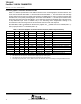
CTL_3_MODE Sub-Address = 0A Read/Write Default = 0x80
7
6 5 4 3 2 1 0
DK[3:1] DKEN RSVD CTL[2:1] RSVD
CTL[2:1]:This read/write register contains the values of the two CTL[2:1] bits that are output on the DVI port during
the blanking interval.
DKEN: This read/write register controls the data deskew enable.
0: Data deskew is disabled, the values in DK[3:1] are not used.
1: Data deskew is enabled, the deskew setting is controlled through DK[3:1].
DK[3:1]: This read/write register contains the deskew setting, each increment adjusts the skew by t
(STEP).
000: Step 1 (minimum setup/maximum hold)
001: Step 2
010: Step 3
011: Step 4
100: Step 5 (default)
101: Step 6
110: Step 7
111: Step 8 (maximum setup/minimum hold)