
Information


TFP401
TFP401A
www.ti.com
SLDS120E –MARCH 2000–REVISED JULY 2013
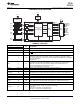
DC ELECTRICAL CHARACTERISTICS
over operating free-air temperature range (unless otherwise noted)
PARAMETER TEST CONDITIONS MIN TYP MAX UNIT
V
ID
Analog input differential voltage
(1)
75 1200 mV
V
IC
Analog input common-mode voltage
(1)
AV
DD
– 300 AV
DD
– 37 mV
V
I(OC)
Open-circuit analog input voltage AV
DD
– 10 AV
DD
+ 10 mV
I
DD(2PIX)
Normal 2-pix/clock power supply current
(2)
ODCK = 82.5 MHz, 2-pix/clock 370 mA
I
PD
Power-down current
(3)
PD = low 10 mA
I
PDO
Output drive power-down current
(3)
PDO = low 35 mA
(1) Specified as dc characteristic with no overshoot or undershoot
(2) Alternating 2-pixel black/2-pixel white pattern. ST = high, STAG = high, QE[23:0] and QO[23:0] C
L
= 10 pF.
(3) Analog inputs are open circuit (transmitter is disconnected from TFP401/401A).
AC ELECTRICAL CHARACTERISTICS
over recommended operating free-air temperature range (unless otherwise noted)
PARAMETER TEST CONDITIONS MIN TYP MAX UNIT
V
ID(2)
Differential input sensitivity
(1)
150 1560 mV
p-p
t
ps
Analog input intra-pair (+ to –) differential skew
(2)
0.4 t
bit
(3)
Analog input inter-pair or channel-to-channel
t
ccs
1 t
pix
(4)
skew
(2)
Worst-case differential input clock jitter
t
ijit
50 ps
tolerance
(2)(5)
ST = low, C
L
= 5 pF 2.4
t
f1
Fall time of data and control signals
(6)(7)
ns
ST = high, C
L
= 10 pF 1.9
ST = low, C
L
= 5 pF 2.4
t
r1
Rise time of data and control signals
(6)(7)
ns
ST = high, C
L
= 10 pF 1.9
ST = low, C
L
= 5 pF 2.4
t
r2
Rise time of ODCK clock
(6)
ns
ST = high, C
L
= 10 pF 1.9
ST = low, C
L
= 5 pF 2.4
t
f2
Fall time of ODCK clock
(6)
ns
ST = high, C
L
= 10 pF 1.9
1 pixel/clock, PIXS = low,
1.8
OCK_INV = low
2 pixel/clock, PIXS = high,
Setup time, data and control signal to falling edge
t
su1
3.8 ns
of ODCK
STAG = high, OCK_INV = low
2 pixel and STAG, PIXS = high,
0.7
STAG = low, OCK_INV = low
1 pixel/clock, PIXS = low,
0.6
OCK_INV = low
Hold time, data and control signal to falling edge of 2 pixel and STAG, PIXS = high,
t
h1
2.5 ns
ODCK STAG = low, OCK_INV = low
2 pixel/clock, PIXS = high,
2.9
STAG = high, OCK_INV = low
(1) Specified as ac parameter to include sensitivity to overshoot, undershoot and reflection.
(2) By characterization
(3) t
bit
is 1/10 the pixel time, t
pix
(4) t
pix
is the pixel time defined as the period of the RxC input clock. The period of ODCK is equal to t
pix
in 1-pixel/clock mode or 2t
pix
when
in 2-pixel/clock mode.
(5) Measured differentially at 50% crossing using ODCK output clock as trigger
(6) Rise and fall times measured as time between 20% and 80% of signal amplitude.
(7) Data and control signals are QE[23:0], QO[23:0], DE, HSYNC, VSYNC. and CTL[3:1].
Copyright © 2000–2013, Texas Instruments Incorporated Submit Documentation Feedback 7
Product Folder Links: TFP401 TFP401A