
Datasheet


7-BitSlave Address
R/
W
8-BitRegister Address(N)
A
8-BitRegisterDataFor
Address(N)
Start Stop
SDA
SCL
7
6
5
4
3
2 1
0
7
6
5
4
3
2 1
0
7
6
5
4
3
2 1
0
7
6
5
4
3
2 1
0
A
8-BitRegisterDataFor
Address(N)
A A
T0035-01
TAS5727
SLOS670 –NOVEMBER 2010
www.ti.com
I
2
C SERIAL CONTROL INTERFACE
The TAS5727 DAP has a bidirectional I
2
C interface that is compatible with the Inter IC (I
2
C) bus protocol and
supports both 100-kHz and 400-kHz data transfer rates for single- and multiple-byte write and read operations.
This is a slave-only device that does not support a multimaster bus environment or wait-state insertion. The
control interface is used to program the registers of the device and to read device status.
The DAP supports the standard-mode I
2
C bus operation (100 kHz maximum) and the fast I
2
C bus operation
(400 kHz maximum). The DAP performs all I
2
C operations without I
2
C wait cycles.
General I
2
C Operation
The I
2
C bus employs two signals, SDA (data) and SCL (clock), to communicate between integrated circuits in a
system. Data is transferred on the bus serially, one bit at a time. The address and data can be transferred in byte
(8-bit) format, with the most-significant bit (MSB) transferred first. In addition, each byte transferred on the bus is
acknowledged by the receiving device with an acknowledge bit. Each transfer operation begins with the master
device driving a start condition on the bus and ends with the master device driving a stop condition on the bus.
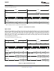
The bus uses transitions on the data pin (SDA) while the clock is high to indicate start and stop conditions. A
high-to-low transition on SDA indicates a start and a low-to-high transition indicates a stop. Normal data-bit
transitions must occur within the low time of the clock period. These conditions are shown in Figure 25. The
master generates the 7-bit slave address and the read/write (R/W) bit to open communication with another
device and then waits for an acknowledge condition. The TAS5727 holds SDA low during the acknowledge clock
period to indicate an acknowledgment. When this occurs, the master transmits the next byte of the sequence.
Each device is addressed by a unique 7-bit slave address plus R/W bit (1 byte). All compatible devices share the
same signals via a bidirectional bus using a wired-AND connection. An external pullup resistor must be used for
the SDA and SCL signals to set the high level for the bus.
Figure 25. Typical I
2
C Sequence
There is no limit on the number of bytes that can be transmitted between start and stop conditions. When the last
word transfers, the master generates a stop condition to release the bus. A generic data transfer sequence is
shown in Figure 25.
The 7-bit address for TAS5715 is 0101 010 (0x54) or 0101 011 (0x56) defined by A_SEL (external pulldown for
0x54 and pullup for 0x56).
Single- and Multiple-Byte Transfers
The serial control interface supports both single-byte and multiple-byte read/write operations for subaddresses
0x00 to 0x1F. However, for the subaddresses 0x20 to 0xFF, the serial control interface supports only
multiple-byte read/write operations (in multiples of 4 bytes).
During multiple-byte read operations, the DAP responds with data, a byte at a time, starting at the subaddress
assigned, as long as the master device continues to respond with acknowledges. If a particular subaddress does
not contain 32 bits, the unused bits are read as logic 0.
During multiple-byte write operations, the DAP compares the number of bytes transmitted to the number of bytes
that are required for each specific subaddress. For example, if a write command is received for a biquad
subaddress, the DAP must receive five 32-bit words. If fewer than five 32-bit data words have been received
when a stop command (or another start command) is received, the received data is discarded.
24 Submit Documentation Feedback Copyright © 2010, Texas Instruments Incorporated
Product Folder Link(s): TAS5727