
Datasheet


26
16
15
OC_ADJ
14
RESET
13
C_STARTUP
12
INPUT_A
11
INPUT_B
10
VI_CM
9
GND
8
AGND
7
VREG
6
INPUT_C
5
INPUT_D
4
FREQ_ADJ
3
OSC_IO+
2
OSC_IO-
1
SD
64-pins QFP package
Pin 1 Marker
White Dot
32
GND_D
31
PVDD_D
30
PVDD_D
29
OUT_D
28
OUT_D
27
BST_D
GVDD_D
25
GVDD_C
24
GND
23
GND
22
NC
21
NC
20
NC
19
NC
18
PSU_REF
17
VDD
33 GND_D
34 GND_C
35
GND_C
36 OUT_C
37 OUT_C
38
PVDD_C
39 PVDD_C
40 BST_C
41
BST_B
42 PVDD_B
43
OUT_B
44
GND_B
45
GND_A
46
47
48
55
49
50
51
READY
52
M1
53
M2
54
M3
GND
56
GND
57
GVDD_B
58
GVDD_A
59
BST_A
60
OUT_A
61
OUT_A
62
PVDD_A
63
PVDD_A
64
GND_A
OTW1
CLIP
PVDD_B
OUT_B
GND_B
DKD PACKAGE
(TOP VIEW)
44 pins PACKAGE
(TOP VIEW)
1
2
3
4
5
6
7
8
9
10
11
12
13
14
15
16
17
18
19
20
21
22
44
43
42
41
40
39
38
37
36
35
34
33
32
31
30
29
28
27
26
25
24
23M3
OC_ADJ
VDD
PSU_REF
M2
M1
READY
OTW
SD
OSC_IO-
OSC_IO+
FREQ_ADJ
INPUT_D
INPUT_C
VREG
AGND
GND
VI_CM
INPUT_B
INPUT_A
C_STARTUP
RESET
GND_C
OUT_A
BST_A
OUT_B
BST_B
PVDD_B
PVDD_A
BST_C
PVDD_C
OUT_C
GND_A
GND_B
OUT_D
PVDD_D
BST_D
GND_D
GVDD_AB
GVDD_CD
PVDD_A
PVDD_D
OUT_D
OUT_A
OTW2
PHD PACKAGE
(TOP VIEW)
Electrical Pin 1
PIN ONE LOCATION PHD PACKAGE
TAS5630B
SLES217C –NOVEMBER 2010–REVISED SEPTEMBER 2012
www.ti.com
These devices have limited built-in ESD protection. The leads should be shorted together or the device placed in conductive foam
during storage or handling to prevent electrostatic damage to the MOS gates.
DEVICE INFORMATION
Terminal Assignment
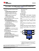
The TAS5630B is available in two thermally enhanced packages:
• 64-Pin QFP (PHD) power package
• 44-Pin PSOP3 package (DKD)
The package types contain heat slugs that are located on the top side of the device for convenient thermal
coupling to the heat sink.
2 Submit Documentation Feedback Copyright © 2010–2012, Texas Instruments Incorporated
Product Folder Links: TAS5630B