
Datasheet


2−16
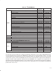
Table 2−2. TAS3103 Clock Default Settings
CLOCK DEFAULT SETTING
SCLKOUT1 SCLKIN
SCLKOUT2 SCLKIN
LRCLK Input
MCLKO MCLKI or XTALI
DAP processing clock Set by pins PLL0 and PLL1
Microprocessor clock Set by pin MICROCLK_DIV
I
2
C sampling clock I
2
C master mode
Microprocessor clock/4
I
2
C slave mode
Microprocessor clock/2
I
2
C master SCL I
2
C sampling clock/90
The selections provided by the dedicated TAS3103 input pins and the programmable settings provided by I
2
C
subaddress commands give the TAS3103 a wealth of clocking options. Table 2−1, in the section describing the serial
audio port (SAP), lists typical clocking selections for different audio sampling rates. However, the following clocking
restrictions must be adhered to:
• MCLKI or XTALI ≥ 128 F
S
(NOTE: For some TDM modes, MCLKI or XTALI must be ≥ 256 F
S
)
• DAP clock ≥ 1400 x F
S
• DAP clock < 136 MHz
• Microprocessor clock/20 ≥ I
2
C SCL clock
• Microprocessor clock ≤ 35 MHz
• I
2
C oversample clock/10 ≥ I
2
C SCL clock
• XTALI ≤ 12.288 MHz
• MCLKI ≤ 25 MHz, unless PLL is bypassed
As long as these restrictions are met, all other clocking options are allowed.
2.3 Controller
The controller serves as the interface between the digital audio processor (DAP), the asynchronous I
2
C bus interface,
and the four general-purpose I/O (GPIO) pins. Included in the controller block is an industry-standard 8051
microprocessor and an I
2
C master/slave bus controller.
2.3.1 8051 Microprocessor
The 8051 microprocessor receives and distributes I
2
C write data, retrieves and outputs to the I
2
C bus controller the
required I
2
C read data, and participates in most processing tasks requiring multiframe processing cycles. The
microprocessor also controls the flow of data into and out of the GPIO pins, which includes volume control when in
the I
2
C master mode The microprocessor has its own data RAM for storing intermediate values and queuing I
2
C
commands, and a fixed program ROM. The microprocessor’s program cannot be altered.
2.3.2 I
2
C Bus Controller
The TAS3103 has a bidirectional, two-wire, I
2
C-compatible interface. Both 100K-bps and 400K-bps data transfer
rates are supported, and the TAS3103 controller can serve as either a master I
2
C device or a slave I
2
C device.
Master/slave operation is defined by the logic level input into pin I2CM_S
(logic 1 = master mode, logic 0 = slave
mode).
If this input level is changed, the TAS3103 must be reset.