
Datasheet


2−15
SCLKIN
OSC
PLL and Clock Management
I2C_SDA
Digital Audio Processor
(DAP)
MCLKO PLL1 PLL0 SCLKOUT1 LRCLK MICROCLK_DIV SCLKOUT2
I2C_SCL
8-Bit
WARP
8051 Microprocessor
1/2
N
1/(M+1)
I
2
C
Master/Slave
Controller
÷10
Master
SCL
MCLKI XTALI XTALO
M
U
X
÷Y = 64
DEFAULT
M
U
X
M
U
X
÷2
÷2
M
U
X
MCLK
PLL
(x11)
M
U
X
÷2
÷2
M
U
X
÷4
M
U
X
Input
SAP
Microprocessor
and
I
2
C Bus Controller
Output
SAP
N = 1 (I
2
C Slave Default)
= 2 (I
2
C Master Default)
I2CM_S
÷ X = 1
DEFAULT
÷ Z = 2
DEFAULT
Oversample Clock
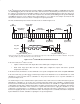
Figure 2−14. DPLL and Clock Management Block Diagram
When the SAP is in the master mode, the serial audio port (SAP) uses the MCLKI/XTALI master clock to drive the
serial port clocks SCLKOUT1, SLCKOUT2, and LRCLK. When the SAP is in the slave mode, LRCLK is an input and
SCLKOUT2 and SCLKOUT1 are derived from SCLKIN. As shown in Figure 2−14, SCLKOUT1 clocks data into the
input SAP and SCLKOUT2 clocks data from the output SAP. Two distinct clocks are required to support TDM to
discrete and discrete to TDM data format conversions. Such format conversions also require that SCLKIN be the
higher valued bit clock frequency. For TDM in/discrete out format conversions, SCLKIN must be equal to the input
bit clock. For discrete in/TDM out format conversions, SCLKIN must be equal to the output bit clock. The frequency
settings for SCLKOUT1, SCLKOUT2, and LRCLK in the SAP master mode, as well as the SAP master/slave mode
selection, are all controlled by I
2
C commands.
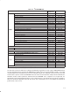
Table 2−2 lists the default settings at power turn on or after a received reset.