
Datasheet


SRC4192, SRC4193
SBFS022B
19
www.ti.com
The bit clock is either an input or output at BCKI (pin 5). In
slave mode, BCKI is configured as an input pin, and may
operate at rates from 32f
S
to 128f
S
,with a minimum of one
clock cycle per data bit. In Master mode, BCKI operates at a
fixed rate of 64f
S
.
The left/right word clock, LRCKI (pin 6), may be configured
as an input or output pin. In Slave mode, LRCKI is an input
pin, while in Master mode LRCKI is an output pin. In either
case, the clock rate is equal to f
S
, the input sampling
frequency. The LRCKI duty cycle is fixed to 50% for Master
mode operation.
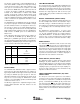
Table 2 illustrates data format selection for the input port. For
the SRC4192, the IFMT0 (pin 10), IFMT1 (pin 11), and
IFMT2 (pin 12) inputs are utilized to set the input port data
format. For the SRC4193, the IFMT[2:0] bits in Control
Register 3 are used to select the data format.
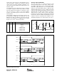
OUTPUT PORT OPERATION
The audio output port is a four-wire synchronous serial
interface that may operate in either Slave or Master mode.
The SDOUT output (pin 23) is the serial audio data output.
Audio data is output at this pin in one of four data formats:
Philips I
2
S, Left Justified, Right Justified, or TDM. The audio
data word length may be 16-, 18-, 20-, or 24-bits. For all word
lengths, the data is triangular PDF dithered from the internal
28-bit data path. The data formats (with the exception of
TDM mode) are shown in Figure 6, while critical timing
parameters are shown in Figure 7 and listed in the Electrical
Characteristics table. The TDM format and timing are shown
in Figures 14 and 15, respectively, while examples of stan-
dard TDM configurations are shown in Figures 16 and 17.
Left Channel
(a) Left Justified Data Format
(b) Right Justified Data Format
Right Channel
LRCKO
BCKO
SDOUT
MSB LSB LSBMSB
LRCKO
BCKO
SDOUT
MSB MSB LSBLSB
(c) I
2
S Data Format
1/f
S
LRCKO
BCKO
SDOUT
MSB LSB MSB LSB
t
SOH
t
DOPD
t
SOL
t
DOH
LRCKO
BCKO
SDOUT
IFMT2 IFMT1 IFMT0 INPUT PORT DATA FORMAT
0 0 0 24-Bit Left Justified
0 0 1 24-Bit I2S
0 1 0 Unused
0 1 1 Unused
1 0 0 16-Bit Right Justified
1 0 1 18-Bit Right Justified
1 1 0 20-Bit Right Justified
1 1 1 24-Bit Right Justified
TABLE 2. Input Port Data Format Selection.
FIGURE 6. Output Data Formats.
FIGURE 7. Output Port Timing.