
Datasheet


SN75LVDS84A, SN65LVDS84AQ
FLATLINK TRANSMITTER
SLLS354E – MAY 1999 – REVISED JANUARY 2001
5
POST OFFICE BOX 655303 • DALLAS, TEXAS 75265
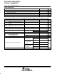
switching characteristics over recommended operating conditions (unless otherwise noted)
PARAMETER TEST CONDITIONS MIN TYP
†
MAX UNIT
t
d0
Delay time, CLKOUT↑ to serial bit
position 0
–0.2 0.2
t
d1
Delay time, CLKOUT↑ to serial bit
position 1
1
7
t
c
0.2
1
7
t
c
0.2
t
d2
Delay time, CLKOUT↑ to serial bit
position 2
2
7
t
c
0.2
2
7
t
c
0.2
t
d3
Delay time, CLKOUT↑ to serial bit
position 3
t
c
= 15.38 ns (± 0.2%),
|Input clock jitter| < 50 ps
‡
, See Figure 6
3
7
t
c
0.2
3
7
t
c
0.2
ns
t
d4
Delay time, CLKOUT↑ to serial bit
position 4
4
7
t
c
0.2
4
7
t
c
0.2
t
d5
Delay time, CLKOUT↑ to serial bit
position 5
5
7
t
c
0.2
5
7
t
c
0.2
t
d6
Delay time, CLKOUT↑ to serial bit
position 6
6
7
t
c
0.2
6
7
t
c
0.2
t
sk(o)
Output skew,
t
n
n
7
t
c
–0.2 0.2 ns
t
d7
Delay time CLKIN↓ to CLKOUT↑
t
c
= 15.38 ns (± 0.2%),
|Input clock jitter| < 50 ps
‡
, See Figure 6
2.7
ns
t
d7
Delay
time
,
CLKIN↓
to
CLKOUT↑
t
c
= 13.33 ns ~ 32.25 ns (± 0.2%),
|Input clock jitter| < 50 ps
‡
, See Figure 6
1 4.5
ns
∆t
()
C cle time o tp t clock jitter
§
t
c
= 15.38 + 0.308 sin (2π500E3t) ± 0.05 ns,
See Figure 7
±62
p
s
∆t
c(o)
C
yc
l
e
ti
me, ou
t
pu
t
c
l
oc
k
jitt
er
§
t
c
= 15.38 + 0.308 sin (2π3E6t) ± 0.05 ns,
See Figure 7
±121
ps
t
w
Pulse duration, high-level output clock
4
7
t
c
ns
t
t
Transition time, differential output voltage
(t
r
or t
f
)
See Figure 3 700 1500 ps
t
en
Enable time, SHTDN↑ to phase lock (Yn
valid)
See Figure 8 1 ms
t
dis
Disable time, SHTDN↓ to off state
(CLKOUT low)
See Figure 9 6.5 ns
†
All typical values are at V
CC
= 3.3 V, T
A
= 25°C.
‡
|Input clock jitter| is the magnitude of the change in the input clock period.
§
Output clock jitter is the change in the output clock period from one cycle to the next cycle observed over 15000 cycles.