
Datasheet


T
CLKIN
EVENDn
ODDDn
t
7
t
0
t
1
t
2
t
3
t
4
t
5
t
6
CLKIN
CLKOUT
Yn
V
OD(L)
0.00V
t
0-6
t
7
1.40V
~2.5V
~0.5V
CLKIN
CLKOUT
or Yn
V
OD(H)
SN75LVDS83A
www.ti.com
SLLS980D –JUNE 2009– REVISED JUNE 2011
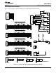
PARAMETER MEASUREMENT INFORMATION (continued)
The worst-case test pattern produces nearly the maximum switching frequency for all of the LVDS outputs.
Figure 6. Worst-Case Power Test Pattern
CLKOUT is shown with CLKSEL at high-level.
CLKIN polarity depends on CLKSEL input level.
Figure 7. SN75LVDS83A Timing Definitions
Copyright © 2009–2011, Texas Instruments Incorporated 11