
Datasheet

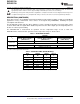


Y
Z
V
OD
R
L
= 54 Ω
A
50 Ω
Signal
Generator
†
C
L
= 50 pF
‡
90%
Output
0 V
10%
t
f
≈ –1.5 V
≈ 1.5 V
t
r
Input 0 V
3 V
t
PHL
1.5 V
t
PLH
†
PRR = 1 MHz, 50% Duty Cycle, t
r
< 6 ns, t
f
< 6 ns, Z
O
= 50 Ω
‡
Includes probe and jig capacitance
SN65LBC174A
SN75LBC174A
SLLS446F –OCTOBER 2000–REVISED OCTOBER 2009
www.ti.com
PARAMETER MEASUREMENT INFORMATION (continued)
Figure 4. Output Switching Test Circuit and Waveforms
6 Submit Documentation Feedback Copyright © 2000–2009, Texas Instruments Incorporated
Product Folder Link(s): SN65LBC174A SN75LBC174A