
Datasheet


www.ti.com
Slave Address
Sink Port Selection Register and Source Plug-In Status Register Description (Sub-Address)
SN75DP129
SLAS583A – JANUARY 2008 – REVISED MARCH 2008
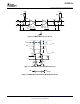
Figure 28. Multiple Byte Read Transfer
Both SDA and SCL must be connected to a positive supply voltage via a pull-up resistor. These resistors should
comply with the I
2
C specification that ranges from 2 k Ω to 19 k Ω . When the bus is free, both lines are high. The
address byte is the first byte received following the START condition from the master device. The 7 bit address is
factory preset to 1000000. Table 2 lists the calls that the SN75DP129 will respond to.
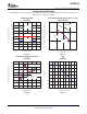
Table 2. SN75DP129 Slave Address
READ/WRITE
FIXED ADDRESS
BIT
BIT 7 (MSB) BIT 6 BIT 5 BIT 4 BIT 3 BIT 2 BIT 1 BIT 0 (R/W)
1 0 0 0 0 0 0 1
The SN75DP129 operates using a multiple byte transfer protocol similar to Figure 28 . The internal memory of the
SN75DP129 contains the phrase DP-HDMI ADAPTOR<EOT> converted to ASCII characters. The internal
memory address registers and the corresponding values can be found in Table 3 .
During a read cycle, the SN75DP129 sends the data (within its selected sub-address) in a single transfer to the
master device requesting the information. See the Reading from the SN75DP129, an Example section of this
data sheet for the proper procedure.
Table 3. SN75DP129 Sink Port and Source Plug-In Status Registers Selection
ADDRESS 0x00 0x01 0x02 0x03 0x04 0x05 0x06 0x07 0x08 0x09 0x0A 0x0B 0x0C 0x0D 0x0E 0x0F 0x10
Data 44 50 2D 48 44 4D 49 20 41 44 41 50 54 4F 52 04 FF
Copyright © 2008, Texas Instruments Incorporated Submit Documentation Feedback 19
Product Folder Link(s): SN75DP129