
Datasheet


www.ti.com
APPLICATION INFORMATION
I
2
C INTERFACE NOTES
SDA
SCL
Start
Condition
Stop
Condition
SDA
SCL
GENERAL I
2
C PROTOCOL
SN75DP129
SLAS583A – JANUARY 2008 – REVISED MARCH 2008
The I
2
C interface can access the internal memory of the SN75DP129. I
2
C is a two-wire serial interface developed
by Philips Semiconductor (see I2C-Bus Specification, Version 2.1, January 2000 ). The bus consists of a data line
(SDA) and a clock line (SCL) with pull-up structures. When the bus is idle, both SDA and SCL lines are pulled
high. All the I
2
C compatible devices connect to the I
2
C bus through open drain I/O pins, SDA and SCL. A master
device, usually a microcontroller or a digital signal processor, controls the bus. The master is responsible for
generating the SCL signal and device addresses. The master also generates specific conditions that indicate the
START and STOP of data transfer. A slave device receives and/or transmits data on the bus under control of the
master device. The SN75DP129 works as a slave and supports the standard mode transfer (100 kbps) as
defined in the I
2
C-Bus Specification.
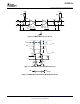
The basic I
2
C start and stop access cycles are shown in Figure 23 .
The basic access cycle consists of the following:
• A start condition
• A slave address cycle
• Any number of data cycles
• A stop condition
Figure 23. I
2
C Start and Stop Conditions
• The master initiates data transfer by generating a start condition. The start condition is when a high-to-low
transition occurs on the SDA line the SCL line is high, as shown in Figure 25 . All I
2
C-compliant devices
should recognize a start condition.
• The master generates the SCL pulses and transmits the 7-bit address and the read/write direction bit R/W on
the SDA line. During all transmissions, the master ensures that data is valid. A valid data condition requires
the SDA line to be stable during the entire high period of the clock pulse (see Figure 24 ). All devices
recognize the address sent by the master and compare it to their internal fixed addresses. Only the slave
device with a matching address generates an acknowledge (see Figure 25 ) by pulling the SDA line low during
the entire high period of the ninth SCL cycle. On detecting this acknowledge, the master knows that a
communication link with a slave has been established.
• The master generates further SCL cycles to transmit data to the slave (R/W bit 0) or receive data from the
slave (R/W bit 1). In either case, the receiver needs to acknowledge the data sent by the transmitter. So an
acknowledge signal can either be generated by the master or by the slave, depending on which one is the
receiver. The 9-bit valid data sequences consisting of 8-bit data and 1-bit acknowledge can continue as long
as necessary (see Figure 26 ).
• To signal the end of the data transfer, the master generates a stop condition by pulling the SDA line from low
to high while the SCL line is high (see Figure 26 ). This releases the bus and stops the communication link
with the addressed slave. All I
2
C compatible devices must recognize the stop condition. Upon the receipt of a
stop condition, all devices know that the bus is released, and they wait for a start condition ,followed by a
matching address.
Copyright © 2008, Texas Instruments Incorporated Submit Documentation Feedback 17
Product Folder Link(s): SN75DP129