
Datasheet


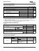


Table Of Contents
- FEATURES
- APPLICATIONS
- DESCRIPTION/ORDERING INFORMATION
- Function Tables
- ABSOLUTE MAXIMUM RATINGS
- RECOMMENDED OPERATING CONDITIONS
- ELECTRICAL CHARACTERISTICS
- DRIVER SECTION
- Electrical Characteristics
- Switching Characteristics
- RECEIVER SECTION
- Electrical Characteristics
- Switching Characteristics
- AUTO-POWERDOWN SECTION
- Electrical Characteristics
- Switching Characteristics
- PARAMETER MEASUREMENT INFORMATION

RECEIVER SECTION
Electrical Characteristics
(1)
Switching Characteristics
(1)
SN65C3243
,
SN75C3243
SLLS353H – JUNE 1999 – REVISED SEPTEMBER 2008 .................................................................................................................................................
www.ti.com
over recommended ranges of supply voltage and operating free-air temperature (unless otherwise noted) (see Figure 6 )
PARAMETER TEST CONDITIONS MIN TYP
(2)
MAX UNIT
V
OH
High-level output voltage I
OH
= – 1 mA V
CC
– 0.6 V
CC
– 0.1 V
V
OL
Low-level output voltage I
OL
= 1.6 mA 0.4 V
V
CC
= 3.3 V 1.6 2.4
V
IT+
Positive-going input threshold voltage V
V
CC
= 5 V 1.9 2.4
V
CC
= 3.3 V 0.6 1.1
V
IT –
Negative-going input threshold voltage V
V
CC
= 5 V 0.8 1.4
V
hys
Input hysteresis (V
IT+
– V
IT –
) 0.5 V
I
off
Output leakage current (except ROUT2B) FORCEOFF = 0 V ± 0.05 ± 10 µ A
r
i
Input resistance V
I
= ± 3 V to ± 25 V 3 5 7 k Ω
(1) Test conditions are C1 – C4 = 0.1 µ F at V
CC
= 3.3 V ± 0.3 V; C1 = 0.047 µ F, C2 – C4 = 0.33 µ F at V
CC
= 5 V ± 0.5 V.
(2) All typical values are at V
CC
= 3.3 V or V
CC
= 5 V, and T
A
= 25 ° C.
over recommended ranges of supply voltage and operating free-air temperature (unless otherwise noted)
PARAMETER TEST CONDITIONS TYP
(2)
UNIT
t
PLH
Propagation delay time, low- to high-level output C
L
= 150 pF, See Figure 3 150 ns
t
PHL
Propagation delay time, high- to low-level output C
L
= 150 pF, See Figure 3 150 ns
t
en
Output enable time C
L
= 150 pF, R
L
= 3 k Ω , See Figure 4 200 ns
t
dis
Output disable time C
L
= 150 pF, R
L
= 3 k Ω , See Figure 4 200 ns
t
sk(p)
Pulse skew
(3)
See Figure 3 50 ns
(1) Test conditions are C1 – C4 = 0.1 µ F at V
CC
= 3.3 V ± 0.3 V; C1 = 0.047 µ F, C2 – C4 = 0.33 µ F at V
CC
= 5 V ± 0.5 V.
(2) All typical values are at V
CC
= 3.3 V or V
CC
= 5 V, and T
A
= 25 ° C.
(3) Pulse skew is defined as |t
PLH
– t
PHL
| of each channel of the same device.
6 Submit Documentation Feedback Copyright © 1999 – 2008, Texas Instruments Incorporated
Product Folder Link(s): SN65C3243 SN75C3243