
Datasheet


1.5 V
V
OH
V
OL
1.5 V
2 V
0.8 VV
OL
+ 0.3 V
t
PZH
t
PHZ
t
PZL
t
PLZ
VOLTAGE WAVEFORMS
Input DE
3 V
0 V
1.5 V1.3 V
C1
C2
C3
R3
R1
R2
0 V
or
3 V
1.5 V
S1
See Note A
TEST CIRCUIT
V
OL
− 0.3 V
Pulse
Generator
50 Ω
See Note B
DE
Output
Output
−2.5 V
2.5 V
V
OL
V
OH
0 V
10%
90%
t
PHL
t
PLH
VOLTAGE WAVEFORMS
R
L
A Input
CC
B Input
Device
Under
Test
C
L
= 50 pF
(see Note A)
S1
TEST CIRCUIT
90%
10%
t
TLH
50%
t
THL
Output
(see Note B)
B Input
A Input = 0 V
50%
R
L
V
CC
Device
Under
Test
C
L
= 50 pF
(see Note A)
S1
TEST CIRCUIT
t
PZL
t
PLZ
0 V
RE Input
1.3 V 1.3 V
GND
0.5 V
Output
V
OH
V
CC
0.5 V
Output
V
OL
50%
50%
t
PZH
t
PHZ
V
ID
= −2.5 V
or 2.5 V
t
PZH
, t
PHZ
Measurement: S1 to GND
t
PZL
, t
PLZ
Measurement: S1 to V
CC
VOLTAGE WAVEFORMS
RE
Input
SN65C1167
SN75C1167, SN65C1168, SN75C1168
www.ti.com
SLLS159F –MARCH 1993–REVISED NOVEMBER 2009
PARAMETER MEASUREMENT INFORMATION (continued)
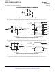
Figure 4. Driver Test Circuit and Voltage Waveforms
G. C
L
includes probe and jig capacitance.
H. The input pulse is supplied by a generator having the following characteristics: PRR = 1 MHz, 50% duty cycle, t
r
= t
f
≤ 6 ns.
Figure 5. Receiver Test Circuit and Voltage Waveforms
I. C
L
includes probe and jig capacitance.
J. The input pulse is supplied by a generator having the following characteristics: PRR = 1 MHz, 50% duty cycle, t
r
= t
f
≤ 6 ns.
Figure 6. Receiver Test Circuit and Voltage Waveforms
Copyright © 1993–2009, Texas Instruments Incorporated Submit Documentation Feedback 9
Product Folder Link(s): SN65C1167 SN75C1167 SN65C1168 SN75C1168