
Datasheet


SN65C1167
SN75C1167, SN65C1168, SN75C1168
SLLS159F –MARCH 1993–REVISED NOVEMBER 2009
www.ti.com
DRIVER SECTION
Electrical Characteristics
(1)
over recommended ranges of supply voltage and operating free-air temperature (unless otherwise noted)
PARAMETER TEST CONDITIONS MIN TYP
(2)
MAX UNIT
V
IK
Input clamp voltage I
I
= −18 mA −1.5 V
V
IL
= 0.8
V
OH
High-level output voltage V
IH
= 2 V, I
OH
= −20 mA 2.4 3.4 V
V,
V
IL
= 0.8
V
OL
Low-level output voltage V
IH
= 2 V, I
OL
= 20 mA 0.2 0.4 V
V,
|V
OD1
| Differential output voltage I
O
= 0 mA 2 6 V
|V
OD2
| Differential output voltage
(1)
2 3.1 V
Change in magnitude of differential
∆|V
OD
| ±0.4 V
output voltage
R
L
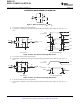
= 100 Ω, See Figure 1
V
OC
Common-mode output voltage ±3 V
Change in magnitude of common-mode
∆|V
OC
| ±0.4 V
output voltage
V
O
= 6 V 100
I
O(OFF)
Output current with power off V
CC
= 0 V µA
V
O
= −0.25 V −100
V
O
= 2.5 V 20
I
OZ
High-impedance-state output current µA
V
O
= 5 V −20
I
IH
High-level input current V
I
= V
CC
or V
IH
1 µA
I
IL
Low-level input current V
I
= GND or V
IL
−1 µA
I
OS
Short-circuit output current
(3)
V
O
= V
CC
or GND, −30 −150 mA
V
I
= V
CC
or GND 4 6
No load,
I
CC
Supply current (total package)
(4)
mA
Enabled
V
I
= 2.4 or 0.5 V 5 3
C
i
Input capacitance 6 pF
(1) Refer to TIA/EIA-422-B for exact conditions.
(2) All typical values are at V
CC
= 5 V, and T
A
= 25°C.
(3) Not more than one output should be shorted at a time, and the duration of the short circuit should not exceed one second.
(4) This parameter is measured per input, while the other inputs are at V
CC
or GND.
Switching Characteristics
over recommended ranges of supply voltage and operating free-air temperature (unless otherwise noted)
PARAMETER TEST CONDITIONS MIN TYP
(1)
MAX UNIT
Propagation delay time, high- to low-level R1 = R2 = 50 Ω, R3 = 500 Ω,
t
PHL
7 12 ns
output C1 = C2 = C3 = 40 pF, S1 is open,
See Figure 2
Propagation delay time, low- to high-level
t
PLH
7 12 ns
output
t
sk(p)
Pulse skew 0.5 4 ns
t
r
Rise time R1 = R2 = 50 Ω, R3 = 500 Ω, 5 10 ns
C1 = C2 = C3 = 40 pF, S1 is open,
t
f
Fall time 5 10 ns
SeeFigure 3
t
PZH
Output enable time to high level R1 = R2 = 50 Ω, R3 = 500 Ω, 10 19 ns
C1 = C2 = C3 = 40 pF, S1 is closed,
t
PZL
Output enable time to low level 10 19 ns
See Figure 4
t
PHZ
Output disable time from low level R1 = R2 = 50 Ω, R3 = 500 Ω, 7 16 ns
C1 = C2 = C3 = 40 pF, S1 is closed,
t
PLZ
Output disable time from high level 7 16 ns
See Figure 4
(1) All typical values are at V
CC
= 5 V, and T
A
= 25°C.
6 Submit Documentation Feedback Copyright © 1993–2009, Texas Instruments Incorporated
Product Folder Link(s): SN65C1167 SN75C1167 SN65C1168 SN75C1168