
Datasheet


SN75976A, SN55976A
9-CHANNEL DIFFERENTIAL TRANSCEIVER
SLLS218B – MAY 1995 – REVISED MAY 1997
11
POST OFFICE BOX 655303 • DALLAS, TEXAS 75265
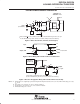
PARAMETER MEASUREMENT INFORMATION
I
O
I
O
V
OD
V
O
V
O
B+
B–
A
I
I
15 pF
15 pF
75 Ω
165 Ω
375 Ω
375 Ω
S1
S2
165 Ω
SN75976A = 5 V
SN55976A = 4.5 V
AB
V
I
Input
(see Note A)
†
†
CDE0 and DE/RE
are at 2 V, BSR is at 0.8 V and, for the SN75976A only, all others are open.
‡
For the SN75976A only, all nine drivers are enabled, similarly loaded, and switching.
Figure 1. Driver Test Circuit, Currents, and Voltages
‡
1.5 V 1.5 V
90% 90%
10%
10%
0V
0V
t
PLH
t
PHL
3 V
0 V
V
OD(H)
V
OD(L)
S1 to A or B
Input
Output, V
OD
t
r
t
f
Figure 2. Driver Delay and Transition Time Test Waveforms
Generator
(see Note A)
Generator
(see Note A)
50 Ω
50 Ω
V
ID
Input B–
I
O
V
O
†
CDE0, CDE1, CDE2, BSR, CRE, and DE/RE at 0.8 V
C
L
= 15 pF
Output
Input B+
†
‡
For the SN75976A only, all nine receivers are enabled and switching.
Figure 3. Receiver Propagation Delay and Transition Time Test Circuit
‡
NOTES: A. All input pulses are supplied by a generator having the following characteristics: t
r
≤ 6 ns, t
f
≤ 6 ns, PRR ≤ 1 MHz, duty cycle = 50%,
Z
O
= 50 Ω.
B. All resistances are in Ω and ± 5%, unless otherwise indicated.
C. All capacitances are in pF and ± 10%, unless otherwise indicated.
D. All indicated voltages are ± 10 mV.