
Datasheet


SCDS087G − APRIL 1999 − REVISED APRIL 2005
4
POST OFFICE BOX 655303 • DALLAS, TEXAS 75265
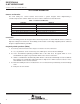
PARAMETER MEASUREMENT INFORMATION
t
PLHREF
t
PHLREF
2.5 V
0 V
2.5 V
V
OL
Input
Tester
VOLTAGE WAVEFORMS
PROPAGATION DELAY TIMES
Output
Reference
TESTER CALIBRATION SETUP (see Note C)
V
OL
Output
Device
Under Test
t
PLHDUT
t
PLH
(see Note D)
t
PHLDUT
t
PHL
(see Note E)
2.5 V
200 kΩ
3.3 V
R
DPU
=
150 Ω
Open-Drain
Test Interface
Motherboard
Interface
2
A1 (V
REF
)
1
GATE
48
B1 (V
BIAS
)
47
V
DPU
TVC16222A
NOTES: A. All input pulses are supplied by generators having the following characteristics: PRR ≤ 10 MHz, Z
O
= 50 Ω, t
r
≤ 2 ns, t
f
≤ 2 ns.
B. The outputs are measured one at a time, with one transition per measurement.
C. Test procedure: t
PLHREF
and t
PHLREF
are obtained by measuring the propagation delay of a reference measuring point.
t
PLHDUT
and t
PHLDUT
are obtained by measuring the propagation delay of the device under test.
D. t
PLH
= t
PLHDUT
− t
PLHREF
E. t
PHL
= t
PHLDUT
− t
PHLREF
B2
46
R
DPU
=
150 Ω
R
DPU
=
150 Ω
R
DPU
=
150 Ω
B3
45
B4
44
B23
25
3
A2 (V
S
)
4
A3 (V
S
)
5
A4 (V
S
)
24
A23 (V
S
)
1.25 V 1.25 V
1.25 V 1.25 V
1.25 V 1.25 V
†† † †
§§ § §
‡
Output tested
Output reference
Input tested
†
‡
§
DEFINITION SYMBOL
GATE
Figure 1. Tester Calibration Setup and Voltage Waveforms