
Datasheet


SN54LVTH245A, SN74LVTH245A
3.3-V ABT OCTAL BUS TRANSCEIVERS
WITH 3-STATE OUTPUTS
SCBS130T − MAY 1992 − REVISED SEPTEMBER 2003
2
POST OFFICE BOX 655303 • DALLAS, TEXAS 75265
description/ordering information (continued)
These devices are designed for asynchronous communication between data buses. They transmit data from
the A bus to the B bus or from the B bus to the A bus, depending on the logic level at the direction-control (DIR)
input. The output-enable (OE
) input can be used to disable the devices so the buses are effectively isolated.
To ensure the high-impedance state during power up or power down, OE should be tied to V
CC
through a pullup
resistor; the minimum value of the resistor is determined by the current-sinking capability of the driver.
Active bus-hold circuitry is provided to hold unused or floating data inputs at a valid logic level. Use of pullup
or pulldown resistors with the bus-hold circuitry is not recommended.
These devices are fully specified for hot-insertion applications using I
off
and power-up 3-state. The I
off
circuitry
disables the outputs, preventing damaging current backflow through the devices when they are powered down.
The power-up 3-state circuitry places the outputs in the high-impedance state during power up and power down,
which prevents driver conflict.
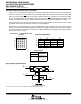
terminal assignments
1234
A A1 DIR V
CC
OE
B A3 B2 A2 B1
C A5 A4 B4 B3
D A7 B6 A6 B5
E GND A8 B8 B7
FUNCTION TABLE
INPUTS
OPERATION
OE DIR
OPERATION
L L B data to A bus
L H A data to B bus
H X Isolation
logic diagram (positive logic)
DIR
OE
A1
B1
To Seven Other Channels
1
2
19
18
Pin numbers shown are for the DB, DW, FK, J, NS, PW, RGY, and W packages.
SN74LVTH245A . . . GQN OR ZQN PACKAGE
(TOP VIEW)
1234
A
B
C
D
E