
Datasheet


SN54LVTH18504A, SN54LVTH182504A, SN74LVTH18504A, SN74LVTH182504A
3.3-V ABT SCAN TEST DEVICES
WITH 20-BIT UNIVERSAL BUS TRANSCEIVERS
SCBS667B – JULY 1996 – REVISED JUNE 1997
28
POST OFFICE BOX 655303 • DALLAS, TEXAS 75265
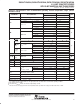
timing requirements over recommended operating free-air temperature range (unless otherwise
noted) (normal mode) (see Figure 14)
SN54LVTH18504A SN74LVTH18504A
V
CC
= 3.3 V
± 0.3 V
V
CC
= 2.7 V
V
CC
= 3.3 V
± 0.3 V
V
CC
= 2.7 V
UNIT
MIN MAX MIN MAX MIN MAX MIN MAX
f
clock
Clock frequency CLKAB or CLKBA 0 100 0 80 0 100 0 80 MHz
t
Pulse duration
CLKAB or CLKBA high or low 4.4 5.6 4.4 5.6
ns
t
w
P
u
lse
d
u
ration
LEAB or LEBA high 3 3 3 3
ns
A before CLKAB↑ or
B before CLKBA↑
2.4 2.8 2.4 2.8
t
su
Setup time
A before LEAB↓ or
CLK high 1.5 0.7 1.5 0.7
ns
su
A
before
LEAB↓
or
B before LEBA↓
CLK low 1.6 1.6 1.6 1.6
CLKEN before CLK↑
2.8 3.4 2.8 3.4
A after CLKAB↑ 1 0.8 1 0.8
t
Hold time
B after CLKBA↑ 1.4 1.1 1.4 1.1
ns
t
h
H
o
ld
ti
me
A after LEAB↓ or B after LEBA↓
3.1 3.5 3.1 3.5
ns
CLKEN after CLK↑
0.7 0.2 0.7 0.2
timing requirements over recommended operating free-air temperature range (unless otherwise
noted) (test mode) (see Figure 14)
SN54LVTH18504A SN74LVTH18504A
V
CC
= 3.3 V
± 0.3 V
V
CC
= 2.7 V
V
CC
= 3.3 V
± 0.3 V
V
CC
= 2.7 V
UNIT
MIN MAX MIN MAX MIN MAX MIN MAX
f
clock
Clock frequency TCK 0 50 0 40 0 50 0 40 MHz
t
w
Pulse duration TCK high or low 9.5 10.5 9.5 10.5 ns
t
St ti
A, B, CLK, CLKEN, LE, or OE
before TCK↑
6.5 7 6.5 7
t
su
Setup time
TDI before TCK↑
2.5 3.5 2.5 3.5
ns
TMS before TCK↑ 2.5 3.5 2.5 3.5
t
Hldti
A, B, CLK, CLKEN, LE, or OE
after TCK↑
1.5 1 1.5 1
t
h
Hold time
TDI after TCK↑
1.5 1 1.5 1
ns
TMS after TCK↑ 1.5 1 1.5 1
t
d
Delay time Power up to TCK↑ 50 50 50 50 ns
t
r
Rise time V
CC
power up 1 1 1 1 µs
PRODUCT PREVIEW information concerns products in the formative or
design phase of development. Characteristic data and other
specifications are design goals. Texas Instruments reserves the right to
change or discontinue these products without notice.