
Datasheet


www.ti.com
Electrical Characteristics
Switching Characteristics
SN74LVC2G53
SINGLE-POLE DOUBLE-THROW (SPDT) ANALOG SWITCH
2:1 ANALOG MULTIPLEXER/DEMULTIPLEXER
SCES324M – JULY 2001 – REVISED FEBRUARY 2007
over recommended operating free-air temperature range (unless otherwise noted)
PARAMETER TEST CONDITIONS V
CC
MIN TYP
(1)
MAX UNIT
I
S
= 4 mA 1.65 V 13 30
V
I
= V
CC
or GND,
I
S
= 8 mA 2.3 V 10 20
V
INH
= V
IL
r
on
On-state switch resistance Ω
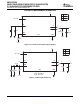
(see Figure 1
I
S
= 24 mA 3 V 8.5 17
and Figure 2 )
I
S
= 32 mA 4.5 V 6.5 13
I
S
= 4 mA 1.65 V 86.5 120
V
I
= V
CC
to GND,
I
S
= 8 mA 2.3 V 23 30
V
INH
= V
IL
r
on(p)
Peak on-state resistance Ω
(see Figure 1
I
S
= 24 mA 3 V 13 20
and Figure 2 )
I
S
= 32 mA 4.5 V 8 15
I
S
= 4 mA 1.65 V 7
V
I
= V
CC
to GND,
I
S
= 8 mA 2.3 V 5
Difference of on-state resistance V
C
= V
IH
∆ r
on
Ω
between switches (see Figure 1
I
S
= 24 mA 3 V 3
and Figure 2 )
I
S
= 32 mA 4.5 V 2
V
I
= V
CC
and V
O
= GND or ± 1
I
S(off)
Off-state switch leakage current V
I
= GND and V
O
= V
CC
, 5.5 V µ A
± 0.1
(1)
V
INH
= V
IH
(see Figure 3 )
± 1
V
I
= V
CC
or GND, V
INH
= V
IL
,
I
S(on)
On-state switch leakage current 5.5 V µ A
V
O
= Open (see Figure 4 )
± 0.1
(1)
± 1
I
I
Control input current V
C
= V
CC
or GND 5.5 V µ A
± 0.1
(1)
I
CC
Supply current V
C
= V
CC
or GND 5.5 V 1 µ A
∆ I
CC
Supply-current change V
C
= V
CC
– 0.6 V 5.5 V 500 µ A
C
ic
Control input capacitance 5 V 3.5 pF
Y 6.5
Switch input/output
C
io(off)
5 V pF
capacitance
COM 10
C
io(on)
Switch input/output capacitance 5 V 19.5 pF
(1) T
A
= 25 ° C
over recommended operating free-air temperature range (unless otherwise noted) (see Figure 5 )
V
CC
= 1.8 V V
CC
= 2.5 V V
CC
= 3.3 V V
CC
= 5 V
FROM TO
± 0.15 V ± 0.2 V ± 0.3 V ± 0.5 V
PARAMETER UNIT
(INPUT) (OUTPUT)
MIN MAX MIN MAX MIN MAX MIN MAX
t
pd
(1)
COM or Y Y or COM 2 1.2 0.8 0.6 ns
t
en
(2)
3.3 9 2.5 6.1 2.2 5.4 1.8 4.5
INH COM or Y ns
t
dis
(3)
3.2 10.9 2.3 8.3 2.3 8.1 1.6 8
t
en
(2)
2.9 10.3 2.1 7.2 1.9 5.8 1.3 5.4
A COM or Y ns
t
dis
(3)
2.1 9.4 1.4 7.9 1.1 7.2 1 5
(1) t
PLH
and t
PHL
are the same as t
pd
. The propagation delay is the calculated RC time constant of the typical on-state resistance of the
switch and the specified load capacitance, when driven by an ideal voltage source (zero output impedance).
(2) t
PZL
and t
PZH
are the same as t
en
.
(3) t
PLZ
and t
PHZ
are the same as t
dis
.
4
Submit Documentation Feedback