
Datasheet


www.ti.com
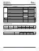
LOGIC DIAGRAM (POSITIVE LOGIC)
1A 1Y
1 6
2A 2Y
3 4
Absolute Maximum Ratings
(1)
SN74LVC2G34-EP
DUAL BUFFER GATE
SCES671 – MARCH 2007
FUNCTION TABLE
(EACH GATE)
INPUT OUTPUT
A Y
H H
L L
over operating free-air temperature range (unless otherwise noted)
MIN MAX UNIT
V
CC
Supply voltage range –0.5 6.5 V
V
I
Input voltage range
(2)
–0.5 6.5 V
V
O
Voltage range applied to any output in the high-impedance or power-off state
(2)
–0.5 6.5 V
V
O
Voltage range applied to any output in the high or low state
(2) (3)
–0.5 V
CC
+ 0.5 V
I
IK
Input clamp current V
I
< 0 V –50 mA
I
OK
Output clamp current V
O
< 0 V –50 mA
I
O
Continuous output current ± 50 mA
Continuous current through V
CC
or GND ± 100 mA
θ
JA
Package thermal impedance
(4)
DCK package 259 ° C/W
T
stg
Storage temperature range –65 150 ° C
(1) Stresses beyond those listed under "absolute maximum ratings" may cause permanent damage to the device. These are stress ratings
only, and functional operation of the device at these or any other conditions beyond those indicated under "recommended operating
conditions" is not implied. Exposure to absolute-maximum-rated conditions for extended periods may affect device reliability.
(2) The input negative-voltage and output voltage ratings may be exceeded if the input and output current ratings are observed.
(3) The value of V
CC
is provided in the recommended operating conditions table.
(4) The package thermal impedance is calculated in accordance with JESD 51-7.
2
Submit Documentation Feedback