
Datasheet


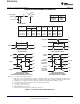

CLR
C
ext
R
ext
/C
ext
R
B
A
Q
1
2
3
7
6
5
SN74LVC1G123
SCES586C –JULY 2004–REVISED OCTOBER 2013
www.ti.com
This integrated circuit can be damaged by ESD. Texas Instruments recommends that all integrated circuits be handled with
appropriate precautions. Failure to observe proper handling and installation procedures can cause damage.
ESD damage can range from subtle performance degradation to complete device failure. Precision integrated circuits may be more
susceptible to damage because very small parametric changes could cause the device not to meet its published specifications.
DESCRIPTION (CONTINUED)
Pulse triggering occurs at a particular voltage level and is not directly related to the transition time of the input
pulse. The A and B inputs have Schmitt triggers with sufficient hysteresis to handle slow input transition rates
with jitter-free triggering at the outputs.
Once triggered, the basic pulse duration can be extended by retriggering the gated low-level-active (A) or high-
level-active (B) input. Pulse duration can be reduced by taking CLR low. CLR can be used to override A or B
inputs. The input/output timing diagram illustrates pulse control by retriggering the inputs and early clearing.
This device is fully specified for partial-power-down applications using I
off
. The I
off
circuitry disables the outputs,
preventing damaging current backflow through the device when it is powered down.
NanoFree™ package technology is a major breakthrough in IC packaging concepts, using the die as the
package.
FUNCTION TABLE
INPUTS
OUTPUTS
Q
CLR A B
L X X L
X H X L
(1)
X X L L
(1)
H L ↑
H ↓ H
↑ L H
(1) These outputs are based on the
assumption that the indicated
steady-state conditions at the A
and B inputs have been set up
long enough to complete any pulse
started before the setup.
Figure 1. LOGIC DIAGRAM (POSITIVE LOGIC)
2 Submit Documentation Feedback Copyright © 2004–2013, Texas Instruments Incorporated
Product Folder Links: SN74LVC1G123