
Datasheet


SCES226I − APRIL 1999 − REVISED MAY 2005
2
POST OFFICE BOX 655303 • DALLAS, TEXAS 75265
description/ordering information (continued)
The ’LV4040A devices are 12-bit asynchronous binary counters with the outputs of all stages available
externally. A high level at the clear (CLR) input asynchronously clears the counter and resets all outputs low.
The count is advanced on a high-to-low transition at the clock (CLK) input. Applications include time-delay
circuits, counter controls, and frequency-dividing circuits.
These devices are fully specified for partial-power-down applications using I
off
. The I
off
circuitry disables the
outputs, preventing damaging current backflow through the devices when they are powered down.
FUNCTION TABLE
(each buffer)
INPUTS
FUNCTION
CLK CLR
FUNCTION
↑ L No change
↓ L Advance to next stage
X H All outputs L
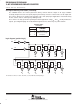
logic diagram (positive logic)
Pin numbers shown are for the D, DB, DGV, J, N, NS, PW, RGY, and W packages.
R
T
R
T
R
T
R
T
R
T
R
T
R
T
R
T
R
T
R
T
R
T
R
T
953
2 4 13 12 14 15 1
11
10
CLR
CLK
Q
A
Q
D
Q
E
Q
H
Q
K
Q
L
Q
F
Q
G
Q
I
Q
J
7
Q
B
6
Q
C