
Datasheet


SCLS298D − JANUARY 1996 − REVISED − OCTOBER 2003
12
POST OFFICE BOX 655303 • DALLAS, TEXAS 75265
APPLICATION INFORMATION
n-bit synchronous counters (continued)
The glitch on RCO is caused because the propagation delay of the rising edge of Q
A
of the second stage is
shorter than the propagation delay of the falling edge of ENT. RCO is the product of ENT, Q
A
, Q
B
, Q
C
, and Q
D
(ENT × Q
A
× Q
B
× Q
C
× Q
D
). The resulting glitch is about 7−12 ns in duration. Figure 3 shows the condition in
which the glitch occurs. For simplicity, only two stages are being considered, but the results can be applied to
other stages. Q
B
, Q
C
, and Q
D
of the first and second stage are at logic one, and Q
A
of both stages are at logic
zero (1110 1110) after the first clock pulse. On the rising edge of the second clock pulse, Q
A
and RCO of the
first stage go high. On the rising edge of the third clock pulse, Q
A
and RCO of the first stage return to a low level,
and Q
A
of the second stage goes to a high level. At this time, the glitch on RCO of the second stage appears
because of the race condition inside the chip.
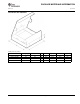
12345
CLK
ENT1
Q
B1
, Q
C1
, Q
D1
Q
A1
RCO1, ENT2
Q
B2
, Q
C2
, Q
D2
Q
A2
RCO2
Glitch (7−12 ns)
Figure 3
The glitch causes a problem in the next stage (stage three) if the glitch is still present when the next rising clock
edge appears (clock pulse 4). To ensure that this does not happen, the clock frequency must be less than the
inverse of the sum of the clock-to-RCO propagation delay and the glitch duration (t
g
). In other words,
f
max
= 1/(t
pd
CLK-to-RCO + t
g
). For example, at 25°C at 4.5-V V
CC
, the clock-to-RCO propagation delay is
43 ns and the maximum duration of the glitch is 12 ns. Therefore, the maximum clock frequency that the
cascaded counters can use is 18 MHz. The following tables contain the f
clock
, t
w
, and f
max
specifications for
applications that use more than two ’HC163 devices cascaded together.