
Datasheet


www.ti.com
APPLICATION INFORMATION
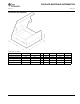
V
CC1
V
CC1
V
CC2
SYSTEM-1 SYSTEM-2
1
2
3
4
8
7
6
5
DIR CTRL
I/O-1
Pullup/Pulldown
or Bus Hold
(1)
V
CC2
I/O-2
Pullup/Pulldown
or Bus Hold
(1)
Enable Times
SN74AVC2T45
DUAL-BIT DUAL-SUPPLY BUS TRANSCEIVER
WITH CONFIGURABLE VOLTAGE TRANSLATION AND 3-STATE OUTPUTS
SCES531J – DECEMBER 2003 – REVISED JUNE 2007
Figure 3 shows the SN74AVC2T45 used in a bidirectional logic level-shifting application. Since the
SN74AVC2T45 does not have an output-enable (OE) pin, the system designer should take precautions to avoid
bus contention between SYSTEM-1 and SYSTEM-2 when changing directions.
Following is a sequence that illustrates data transmission from SYSTEM-1 to SYSTEM-2 and then from
SYSTEM-2 to SYSTEM-1.
STATE DIR CTRL I/O-1 I/O-2 DESCRIPTION
1 H Out In SYSTEM-1 data to SYSTEM-2
SYSTEM-2 is getting ready to send data to SYSTEM-1. I/O-1 and I/O-2 are
2 H Hi-Z Hi-Z disabled.
The bus-line state depends on pullup or pulldown.
(1)
DIR bit is flipped. I/O-1 and I/O-2 still are disabled.
3 L Hi-Z Hi-Z
The bus-line state depends on pullup or pulldown.
(1)
4 L In Out SYSTEM-2 data to SYSTEM-1
(1) SYSTEM-1 and SYSTEM-2 must use the same conditions, i.e., both pullup or both pulldown.
Figure 3. Bidirectional Logic Level-Shifting Application
Calculate the enable times for the SN74AVC2T45 using the following formulas:
• t
PZH
(DIR to A) = t
PLZ
(DIR to B) + t
PLH
(B to A)
• t
PZL
(DIR to A) = t
PHZ
(DIR to B) + t
PHL
(B to A)
• t
PZH
(DIR to B) = t
PLZ
(DIR to A) + t
PLH
(A to B)
• t
PZL
(DIR to B) = t
PHZ
(DIR to A) + t
PHL
(A to B)
In a bidirectional application, these enable times provide the maximum delay from the time the DIR bit is
switched until an output is expected. For example, if the SN74AVC2T45 initially is transmitting from A to B, then
the DIR bit is switched; the B port of the device must be disabled before presenting it with an input. After the B
port has been disabled, an input signal applied to it appears on the corresponding A port after the specified
propagation delay.
15
Submit Documentation Feedback