
Datasheet


www.ti.com
DESCRIPTION/ORDERING INFORMATION (CONTINUED)
B1
DIR
5
7
A1
2
V
CCA
V
CCB
B2
6
A2
3
SN74AVC2T45
DUAL-BIT DUAL-SUPPLY BUS TRANSCEIVER
WITH CONFIGURABLE VOLTAGE TRANSLATION AND 3-STATE OUTPUTS
SCES531J – DECEMBER 2003 – REVISED JUNE 2007
The SN74AVC2T45 is designed for asynchronous communication between two data buses. The logic levels of
the direction-control (DIR) input activate either the B-port outputs or the A-port outputs. The device transmits
data from the A bus to the B bus when the B-port outputs are activated and from the B bus to the A bus when
the A-port outputs are activated. The input circuitry on both A and B ports always is active and must have a logic
HIGH or LOW level applied to prevent excess I
CC
and I
CCZ
.
The SN74AVC2T45 is designed so that the DIR input is powered by V
CCA
.
This device is fully specified for partial-power-down applications using I
off
. The I
off
circuitry disables the outputs,
preventing damaging current backflow through the device when it is powered down.
The V
CC
isolation feature ensures that if either V
CC
input is at GND, both ports are in the high-impedance state.
NanoFree™ package technology is a major breakthrough in IC packaging concepts, using the die as the
package.
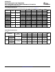
FUNCTION TABLE
(1)
(EACH TRANSCEIVER)
INPUT
OPERATION
DIR
L B data to A bus
H A data to B bus
(1) Input circuits of the data I/Os always are active.
LOGIC DIAGRAM (POSITIVE LOGIC)
(1)
(1) Pin numbers are for the DCT and DCU packages only.
2
Submit Documentation Feedback