
Datasheet


www.ti.com
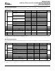
To Seven Other Channels
1DIR
1A1
1B1
1OE
To Seven Other Channels
2DIR
2A1
2B1
2OE
1
47
24
36
48
2
25
13
Absolute Maximum Ratings
(1)
SN74ALVC164245
16-BIT 2.5-V TO 3.3-V/3.3-V TO 5-V LEVEL-SHIFTING TRANSCEIVER
WITH 3-STATE OUTPUTS
SCAS416P – MARCH 1994 – REVISED NOVEMBER 2005
LOGIC DIAGRAM (POSITIVE LOGIC)
over operating free-air temperature range for V
CCB
at 5 V and V
CCA
at 3.3 V (unless otherwise noted)
MIN MAX UNIT
V
CCA
–0.5 4.6
V
CC
Supply voltage range V
V
CCB
–0.5 6
Except I/O ports
(2)
–0.5 6
V
I
Input voltage range I/O port A
(3)
–0.5 V
CCA
+ 0.5 V
I/O port B
(2)
–0.5 V
CCB
+ 0.5
I
IK
Input clamp current V
I
< 0 –50 mA
I
OK
Output clamp current V
O
< 0 –50 mA
I
O
Continuous output current ± 50 mA
Continuous current through each V
CC
or GND ± 100 mA
DGG package 70
DL package 63
θ
JA
Package thermal impedance
(4)
° C/W
GQL/ZQL package 42
GRD/ZRD package 36
T
stg
Storage temperature range –65 150 ° C
(1) Stresses beyond those listed under "absolute maximum ratings" may cause permanent damage to the device. These are stress ratings
only, and functional operation of the device at these or any other conditions beyond those indicated under "recommended operating
conditions" is not implied. Exposure to absolute-maximum-rated conditions for extended periods may affect device reliability.
(2) This value is limited to 6 V maximum.
(3) This value is limited to 4.6 V maximum.
(4) The package thermal impedance is calculated in accordance with JESD 51-7.
3