
Datasheet


SN54ALS161B, SN54ALS162B, SN54ALS163B, SN54AS161, SN54AS163
SN74ALS161B, SN74ALS163B, SN74AS161, SN74AS163
SYNCHRONOUS 4-BIT DECADE AND BINARY COUNTERS
SDAS276A – DECEMBER 1994 – REVISED JULY 2000
11
POST OFFICE BOX 655303 • DALLAS, TEXAS 75265
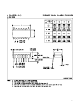
PARAMETER MEASUREMENT INFORMATION
SERIES 54ALS/74ALS AND 54AS/74AS DEVICES
t
PLZ
t
PHL
t
PLH
0.3 V
t
PZL
t
PLH
t
PHL
LOAD CIRCUIT
FOR 3-STATE OUTPUTS
From Output
Under Test
Test
Point
S1
C
L
= 50 pF
(see Note A)
7 V
3 V
3 V
0 V
0 V
t
h
t
su
VOLTAGE WAVEFORMS
SETUP AND HOLD TIMES
Timing
Input
Data
Input
3 V
3 V
0 V
0 V
High-Level
Pulse
Low-Level
Pulse
t
w
VOLTAGE WAVEFORMS
PULSE DURATIONS
Input
Out-of-Phase
Output
(see Note C)
3 V
3 V
0 V
0 V
V
OL
V
OH
V
OH
V
OL
Output
Control
(low-level
enabling)
Waveform 1
S1 Closed
(see Note B)
Waveform 2
S1 Open
(see Note B)
≈0 V
V
OH
V
OL
≈3 V
In-Phase
Output
0.3 V
VOLTAGE WAVEFORMS
PROPAGATION DELAY TIMES
VOLTAGE WAVEFORMS
ENABLE AND DISABLE TIMES, 3-STATE OUTPUTS
V
CC
Test
Point
From Output
Under Test
C
L
= 50 pF
(see Note A)
LOAD CIRCUIT
FOR OPEN-COLLECTOR OUTPUTS
LOAD CIRCUIT FOR
BI-STATE TOTEM-POLE OUTPUTS
From Output
Under Test
Test
Point
C
L
= 50 pF
(see Note A)
500 Ω
500 Ω
500 Ω
500 Ω
1.5 V
1.5 V 1.5 V
1.5 V
1.5 V
1.5 V 1.5 V
t
PHZ
t
PZH
1.5 V 1.5 V
1.5 V
1.5 V
1.5 V 1.5 V
1.5 V 1.5 V
1.5 V 1.5 V
NOTES: A. C
L
includes probe and jig capacitance.
B. Waveform 1 is for an output with internal conditions such that the output is low except when disabled by the output control.
Waveform 2 is for an output with internal conditions such that the output is high except when disabled by the output control.
C. When measuring propagation delay items of 3-state outputs, switch S1 is open.
D. All input pulses have the following characteristics: PRR ≤ 1 MHz, t
r
= t
f
= 2 ns, duty cycle = 50%.
E. The outputs are measured one at a time with one input transition per measurement.
Figure 1. Load Circuits and Voltage Waveforms