
Datasheet


TG
C
C
TG
C
TG
C
C
C
C
TG
C
C
PRE
CLK
D
CLR
Q
Q
C
SN54AHCT74
SN74AHCT74
SCLS263O –OCTOBER 1995–REVISED JUNE 2013
www.ti.com
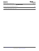
LOGIC DIAGRAM, EACH FLIP-FLOP (POSITIVE LOGIC)
ABSOLUTE MAXIMUM RATINGS
over operating free-air temperature range (unless otherwise noted)
(1)
VALUE UNIT
Supply voltage range, V
CC
–0.5 to 7 V
Input voltage range, V
I
(2)
–0.5 to 7 V
Output voltage range, V
O
(2)
–0.5 to V
CC
+ 0.5 V
Input clamp current, I
IK
(V
I
< 0) –20 mA
Output clamp current, I
OK
(V
O
< 0 or V
O
> V
CC
) ±20 mA
Continuous output current, I
O
(V
O
= 0 to V
CC
) ±25 mA
Continuous current through V
CC
or GND ±50 mA
D package
(3)
86
DB package
(3)
96
DGV package
(3)
127
Package thermal impedance, θ
JA
N package
(3)
80 °C/W
NS package
(3)
76
PW package
(3)
113
RGY package
(4)
47
Storage temperature range, T
stg
–65 to 150 °C
(1) Stresses beyond those listed under “absolute maximum ratings” may cause permanent damage to the device. These are stress ratings
only, and functional operation of the device at these or any other conditions beyond those indicated under “recommended operating
conditions” is not implied. Exposure to absolute-maximum-rated conditions for extended periods may affect device reliability.
(2) The input and output voltage ratings may be exceeded if the input and output current ratings are observed.
(3) The package thermal impedance is calculated in accordance with JESD 51-7.
(4) The package thermal impedance is calculated in accordance with JESD 51-5
2 Submit Documentation Feedback Copyright © 1995–2013, Texas Instruments Incorporated
Product Folder Links: SN54AHCT74 SN74AHCT74