
Datasheet


www.ti.com
t
c(n)
1/f0
Period Jitter
Peak to Peak Jitter
1/f0
PRBS INPUT
OUTPUT
CLOCK INPUT
IDEAL
OUTPUT
ACTUAL
OUTPUT
t
jit(per)
= t
c(n)
-1/f0
t
jit(pp)
V
A
-V
B
INPUTS
V
A
-V
B
0.2 V - Type 1
0.4 V - Type 2
V
IC
1 V
V
OH
V
CC
/2
V
OL
V
OH
V
OL
V
CC
/2
V
OH
V
OL
V
CC
/2
V
A
V
B
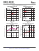
PIN ASSIGNMENTS
SN65MLVD203D (Marked as MLVD203)
SN65MLVD207D (Marked as MLVD207)
(TOP VIEW)
1
2
3
4
5
6
7
14
13
12
11
10
9
8
NC
R
RE
DE
D
GND
GND
V
CC
V
CC
A
B
Z
Y
NC
NC - No internal connection
1
2
3
4
8
7
6
5
R
RE
DE
D
V
CC
B
A
GND
SN65MLVD201D (Marked as MF201)
SN65MLVD206D (Marked as MF206)
(TOP VIEW)
SN65MLVD201 , SN65MLVD203
SN65MLVD206 , SN65MLVD207
SLLS558C – DECEMBER 2002 – REVISED JANUARY 2007
A. All input pulses are supplied by an Agilent 8304A Stimulus System.
B. The measurement is made on a TEK TDS6604 running TDSJIT3 application software
C. Period jitter is measured using a 100 MHz 50 1% duty cycle clock input.
D. Peak-to-peak jitter is measured using a 200 Mbps 2
15
-1 PRBS input.
Figure 12. Receiver Jitter Measurement Waveforms
12 Submit Documentation Feedback Copyright © 2002 – 2007, Texas Instruments Incorporated
Product Folder Link(s): SN65MLVD201 SN65MLVD203 SN65MLVD206 SN65MLVD207